This thread has been locked.

If you have a related question, please click the "Ask a related question" button in the top right corner. The newly created question will be automatically linked to this question.

TPS61022: Boost converted not getting enough output current

Part Number: TPS61022

Hello,

I am designing a boost circuit based around the tps61022 chip.

My requirements: 

Single cell lipo (3.7v) to boost to 5V 3A (aprox 2.4 amps or so, burst for aprox 2 or less seconds when used with LED)

It is used for a high power LED light with a micro controller .

I used the workbench design tool.

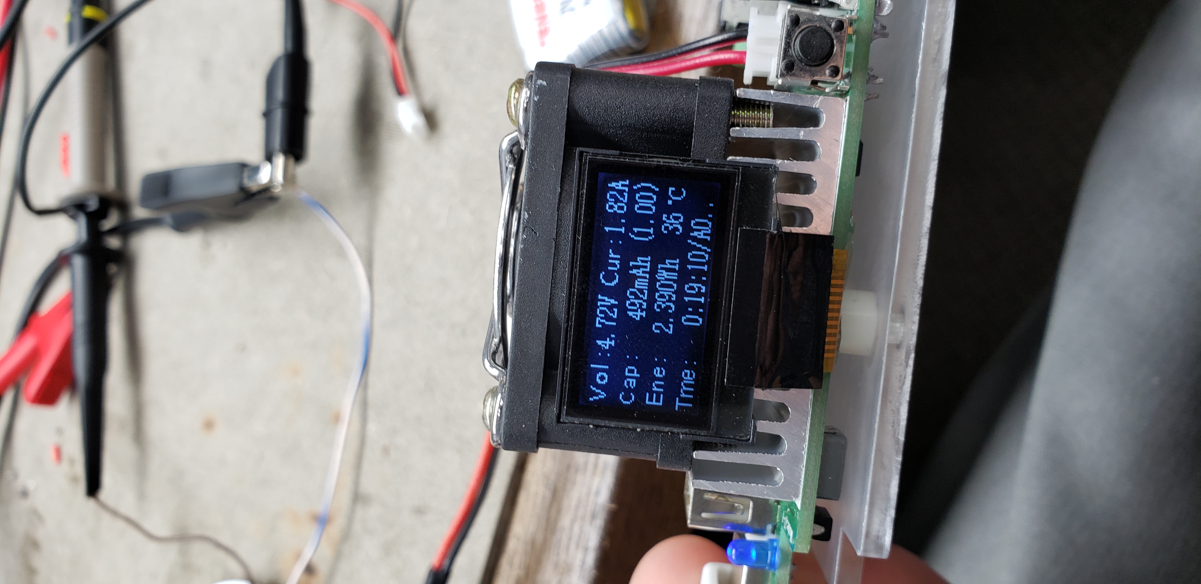
During my testing bench supply as a input at 3.7v. I was able to only get about maybe 1 amp output with the output dropping down to 4.8v (drawing more current would result in the boost chip dying).

I was directed to this help page from the support page.

The components used:

TPS61022

Inductor: SRN8040-1R0Y (digikey  part: SRN8040-1R0YCT-ND)

732K resistor: ERJ-2RKF7323X (digi part: P732KLCT-ND)

100K resistor: ERJ-2RKF1003X (digi part: P100KLCT-ND)

Input cap QTY 2: 10uf (CL21A226MOCLRNC, digi part: 1276-6780-1-ND)
Output cap QTY 2: 22uf CL21A226MOCLRNCm digi part: 1276-6780-1-ND

I did try adding a 470uf electrolytic cap, that did not solve my issue.

Speaking to the help person in the original ticket, he suggest to use the parts mention in the datasheet (mainly the inductor).

I have ordered some parts to try and solve the issue:

Inductor as per datasheet: XAL7030-102MEC 

10uf ceramic cap, C0805C106K8PACTU

22uf ceramic cap, GRM188R61A226ME15D

47uf ceramic cap, GRM31CR61A476KE15L


As well these are some of my calculation from the datasheet:

Iout(CL) Vin 3.7 V
Equation 5 IL (DC) 3.649 A Vout 5 V
Equation 2 Duty cycle (D) 0.334 % Iout 3 A
Equation 6 IL (P-P) 1.236 A fsw 1 MHz
Equation 7 IL(P) 4.267 n(power conversion efficiency) 90%
Equation 9 Vripple(ESR) Inductor inductance 1 uH


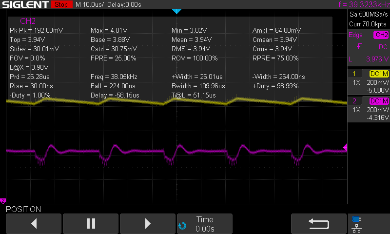
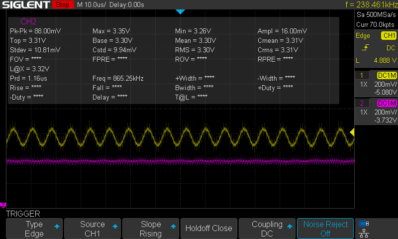
Also some scope references:

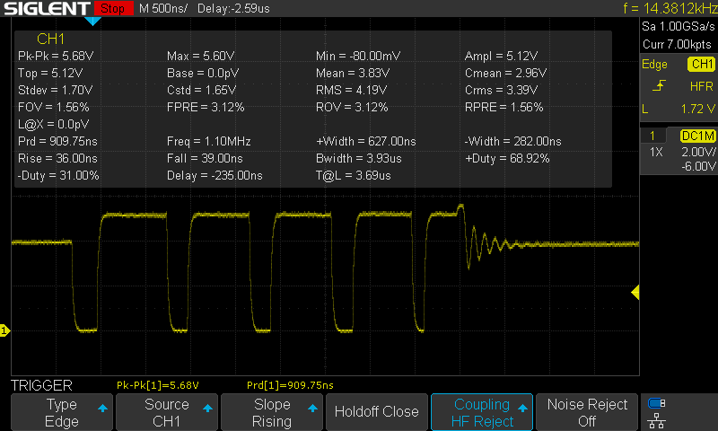
Measuring inductor at 600 mah load:


Inductor at no load:


Output no load:

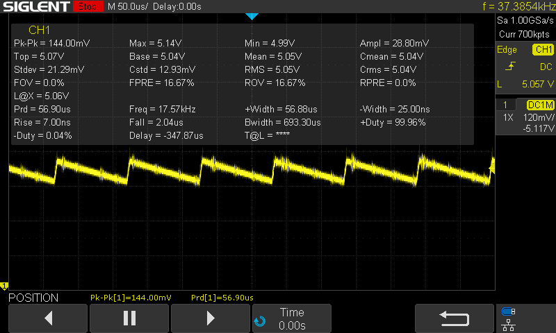
Output at 1 amp load


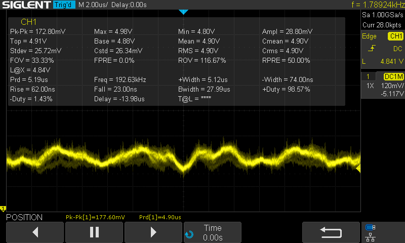
This last screen cap is not great (was from last week not sure if it was accurate/labeled correctly), I can redo it tomorrow when I get the new parts in.

In the mean time:

Did I miss something or miscalculate something?

Any possible idea on why the low output?

  • Hi Vismantas,

    The components you selected look good. Can you share the layout? 

  • Hello, thanks for you help.

    Here is the top and bottom layers of my board.

  • Just a update:

    So the new parts have arrived.

    While technically my light ring (this circuit device) is stable and output the correct light output in bursts(in lux). It technically works now.

    But testing with my usb load tester I am only able to pull roughly 1.8 amps with the output dropping to about 4.7V (I did not want to go higher on the test load at this time in case the chip dies).

    What would be your suggestion on getting my wanted output of around 2.4 - 3 amps output at 5v?

    The updated components list from mouser used in the circuit:

    10 uf input cap (C0805C106K8PACTU)

    22 uf input cap (GRM188R61A226ME15D)

    TPS61022RWUR (same boost chip)

    QTY 2:  47uf output cap GRM31CR61A476KE15L

    inductor XAL7030-102MEC (as listed in datasheet)


    One note I did add an extra 470uf electrolytic cap on the input during the test. And I ran this off a lipo battery not my bench PSU, I have tested with my bench PSU and the results are the same so the battery is not a limitation.

    Here are also some screen shots with the 1.8A load. ch1 Yellow is output, ch2 pink is input


    No load:

    Load at 1.8A with usb tester:

  • Hi Vismantas,

    Thank you for providing so many information. It's very helpful.

    The inductor, output caps, input caps, input electrolytic caps are all good choice. The top layer layout is good but the bottom layout GND is bad.

    Below picture is how current flow when TPS61022 is switching. When TPS61022 low side switch turns on, current flows from input caps positive pad, inductor, IC SW pin, low side switch, IC GND pin, input caps GND pad. You could see the bottom layer GND trace is too thin to handle so big current. The thin trace will cause high voltage drop, may cause inaccurate voltage feedback. That's why you see at high load current the Vout decreases.  

    So please place a wide GND polygon at bottom layer in next version PCB.

    You can do s simple test. Solder a short, wide wire between output caps COUT3 GND pad and input caps CIN4 GND pad.

  • Thank you for the suggestion, That does make sense.

    Just a quick note, I did a quick test this morning using a short piece of cat 5 cable (24 awg I think) and there did not seem to be an improvement, same amount of current. I will take a look further into it.

  • Hi Vismantas,

    One more thing, how do you measure the output voltage? Please make sure use DMM to measure Vout directly close to output capacitor. Because the thin GND trace has big voltage drop at high load current.

  • Hi Zack,

    Sorry for the late reply.

    Yes I did use a DMM to measure at the V5 pin.

    I have made some changes and tried to follow more closely to the recommended layout design.

    Could you take a look and see if there is any more recommendation you could make before reordering a sample board?

    Some notes:

    The ground rail 1.5MM tick, my board is a 4 layer board so I Made this trace equal on all 4 layers with a some via's.

    The +5v output rail is 2mm thick and runs on 3 layers top, bottom and one inner layer.

    Thank you.

  • Hi Vismantas,

    The layout is better than last one:)

    TPS61022 recommended effective output capacitance range bigger than 30uF shown in datasheet page 4.Could you tell the output capacitors part number? I can help check the effective output capacitance for you.

    Since the lipo battery range is 3.0V-4.2V, during switching. The maximum input average current would go up to 5-6A. The 1.5MM thick gound is not wide enough. We would suggest set the second layer all GND. And put some via close to Cin cap GND pad.

  • Zack,

    The output caps I am using are 2x Samsung 22uf 16v X5R caps.

    Man. part num: CL21A226MOCLRNC

    Digi key part: 1276-6780-1-ND

    What would be the calculation for effective output capacitance? 

    I will also try to make a layer with all ground.

  • Hi,

    Normally the ceramic capacitor datasheet would provide the DC bias characteristics curve for customers. I searched the samsung electronics but cannot find this data. I prefer using murata and TDK's capacitor because they could provide the DC bias characteristics curve.

    The effective capacitance cannot be calculated. You need to inquiry this value from Samsung. Or use another one.

    TPS61022 EVM user's guide has recommended output capacitors. It uses 3 * 0805 22uF 10V caps. They have been tested and verified.