This thread has been locked.

If you have a related question, please click the "Ask a related question" button in the top right corner. The newly created question will be automatically linked to this question.

UCC27211

Other Parts Discussed in Thread: UCC27211

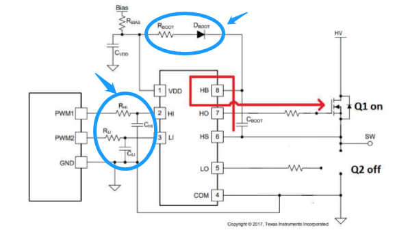
I now use the UCC27211 driver chip to complete the driver task. However, the rising and falling edges of the drive signal reached nearly 100 ns. My bootstrap capacitor and Vcc capacitor are close to the chip pins, and the values are 0.1u and 1u, respectively. I tried to use 1u and 4.7u respectively, but it still has the same effect as before. What should I do? Thank you.

  • Hi Dailing, 

    Sorry that you're still having issues with our devices. 

    Can you please confirm the following?

    1. MOSFETs PN to verify bootstrap capacitor sizing. 

    2. VHB_HS( are you still seeing 1V?), VHS_GND, VDD(I believe you mentioned that this is 12V, please confirm on driver's pin)

    The copied app note should be a good starting point to estimate bootstrap components sizing.

    https://www.ti.com/lit/an/slua887/slua887.pdf

    Thanks again for your interest in our drivers.

    Regards,

    -Mamadou

  • Hello, thank you for your answer, but there are still some questions I would like to ask you.
    1. The chip can work normally, and the voltage value of the related pin is also normal, but the rising and falling edges are too slow;
    2. For the problem of slow rising and falling edges, can you solve the problem by changing the bootstrap capacitor and its related loop?

  • Hello, and I checked the relevant loop in the pdf file you sent me. I found that there is no component in the two circles shown in the figure below. Does this have any effect?
    In addition, I adjusted the size of the bootstrap capacitor according to the calculation formula, but the rising and falling edges still have not improved, and it is the same.
  • Hello Dailing,

    I work with Mamadou supporting this device. I have a couple of questions/comments regarding your concern.

    The Vgs rising and falling time can be affected by a few parameters such as Qg, or total gate charge of the MOSFET, gate resistance, and the board layout trace inductance of the gate drive loop can affect the rising and falling times.

    Can you provide the MOSFET part numbers you are using? And the gate resistance? Also if you have the PCB layout of the driver and power devices we can review and comment.

    Regards,

  • MOS:CSD18534

    Rg:10R

    Driver:UCC27211

  • Hello Dailing,

    CSD18534 has a 17nC gate charge @ 10V Vgs that roughly equates to Cgate = 17nC / 12V = 1.416nF.

    Cboot must be >= 10*Cgate ~= 100nF for sufficient margin.

    CVcc must be >= 10*Cboot ~= 2uF 

    RC Filter in input stage is optional assuming you have optimized PCB layout.

    Dboot (with Vbus minimum voltage ratings) on the PDF file is a must as it blocks high-side charging current from reaching the supply and allows the path in red and provides current path for charging boot capacitor (path in blue).

    Please reduce gate resistance to 1 or 2 Ohms and retake measurements.

    Please let us know if you still trouble with your design.

    Regards,

    -Mamadou