Other Parts Discussed in Thread: TIDA-01540, UCC21220
Hi Experts,
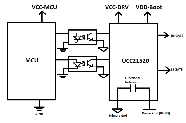
I'm using UCC21520 to drive one leg of a 3phase inverter. The block diagram of the system is -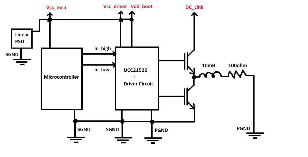
SCHEMATIC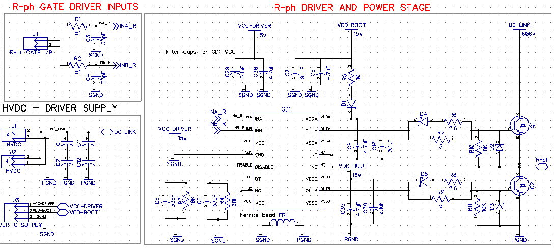
The high side and low side gate pulses are perfect when no load is attached and DC-link = 0 V. At no load, as DC-Link is increased, beyond 30v, I start hearing a strange hum from the gate-source loop. I'm unable to discern the cause, but this phenomena happens in other phases too. The amplitude of the hum increases as DC-Link increases. It sounds like a HF sine signal.
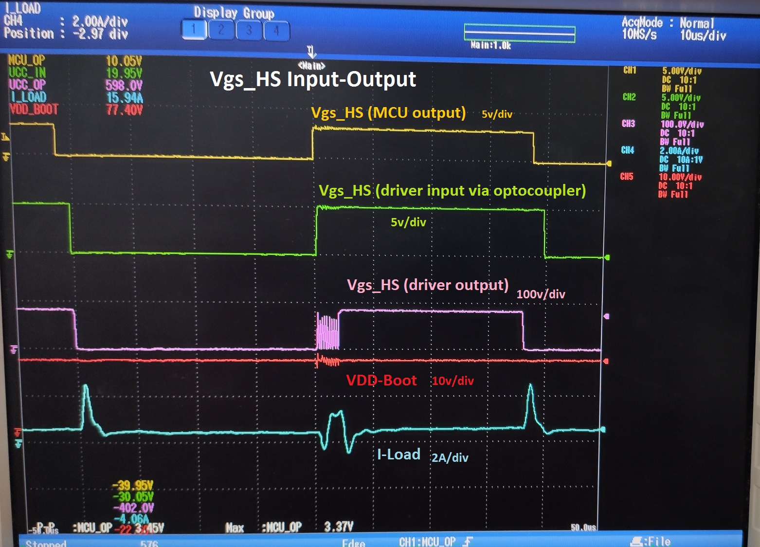
Things changes drastically when load is attached. At ~30v DC link, 10mh+100ohm RL load, the high side gate pulses get distorted, rapidly switching between high and low in the turn-on duration -

Vg_high is referenced wrt GND.
This phenomenon occurs only during High Side turn on.
Zooming in on the waveforms.
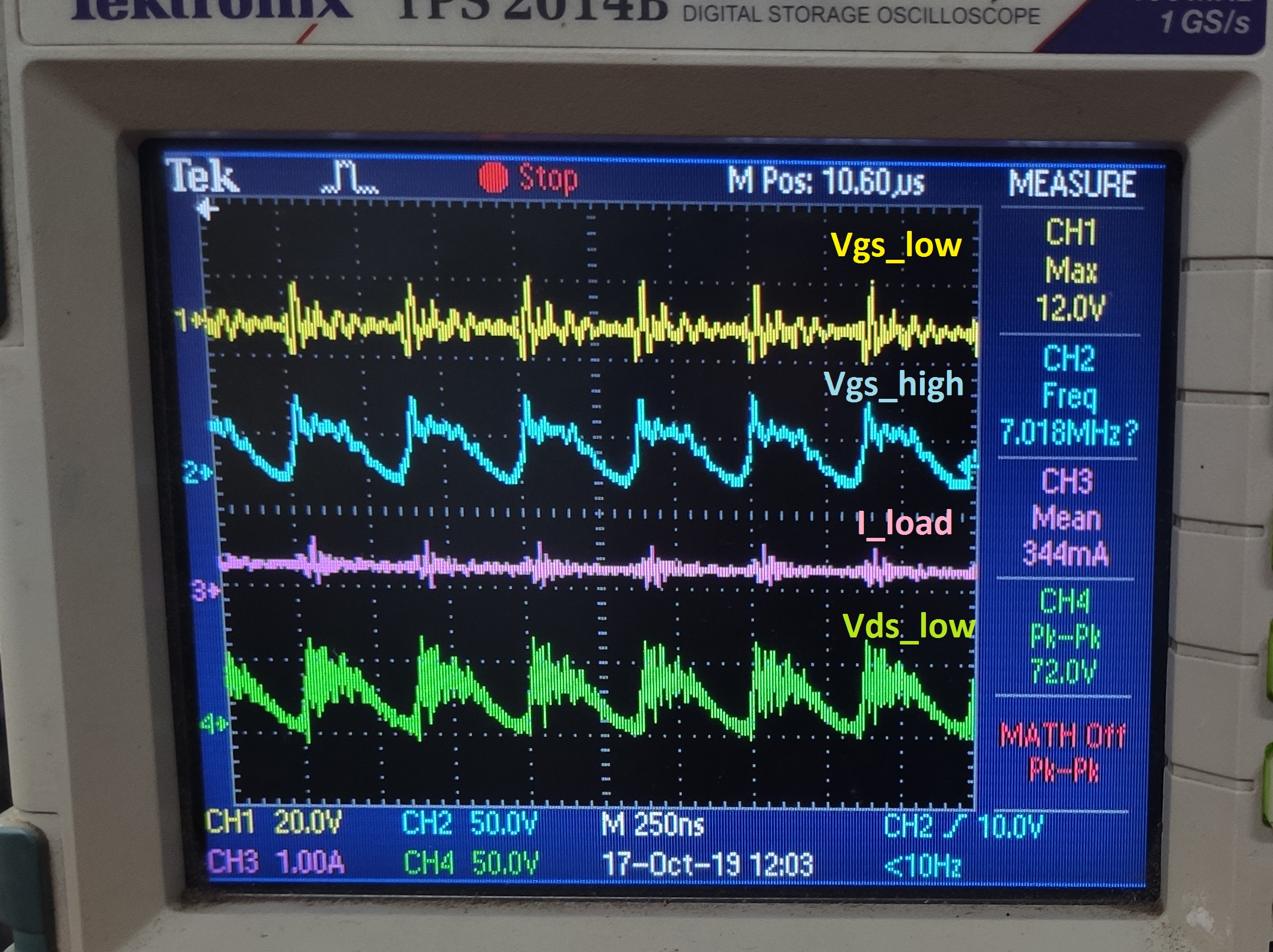
This distortion occured at 30v DC-Link, 100ohm+10mH load. As load resistance is increased, distortion occurs at higher levels of DC-Link (does this have something to do with load current, di/dt issues maybe?)
Surprisingly, the same distortion gets reflected at the MCU side. The supply of the MCU gets distorted in the same manner. I tried changing to a new MCU board, put in bypass capacitors on MCU's LDO and VCC pin, but the problem still persists. (so, maybe the output stage of the driver itself is causing the problem?)
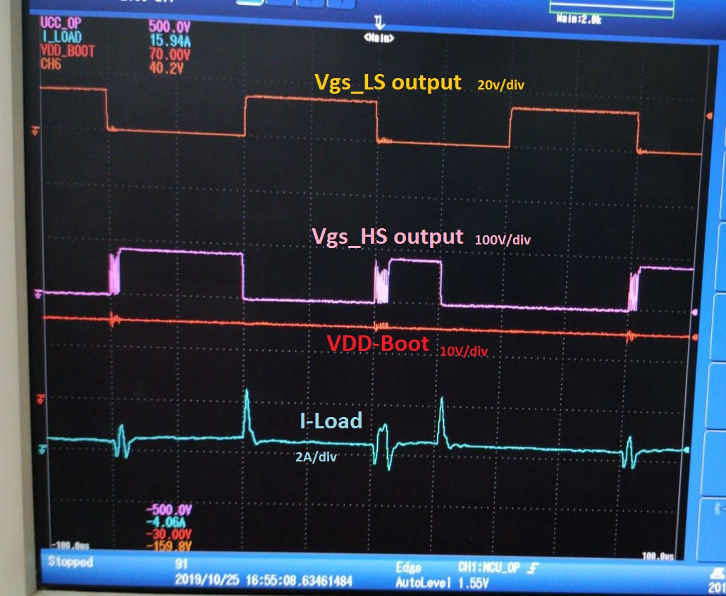
Out of curiosity, I increased the DC_Link further. The hum intensity kept on increasing with DC-Link and at one point, the hum stopped and suddenly the driver started behaving weirdly like this -
(Colour scheme is changed here, sorry)
YELLOW = HIGH SIDE (wrt to gnd)
BLUE = LOW SIDE (wrt gnd)
Even after multiple resets, the driver now always produces high side gate pulses in the fashion shown in the video. And now, this thing happens at DC-Link <15v, for load = 100ohm + 10mH. In the same turn-on period, the driver initially produces proper high side gate pulses and then just fails for the remaining duration of the on-time. This occurs periodically and only at the HIGH SIDE. Low side pulses are perfect!
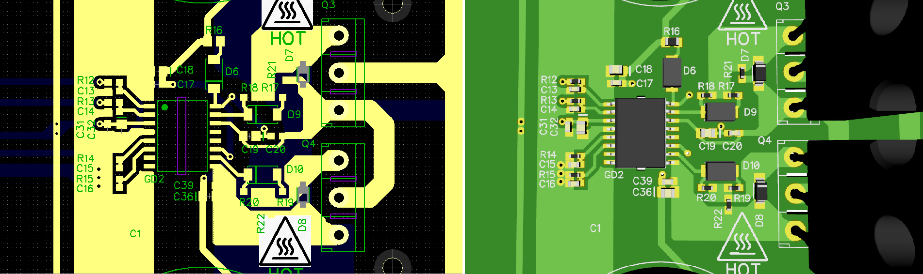
Here is a snippet from my board layout -
GATE-SOURCE LAYOUT
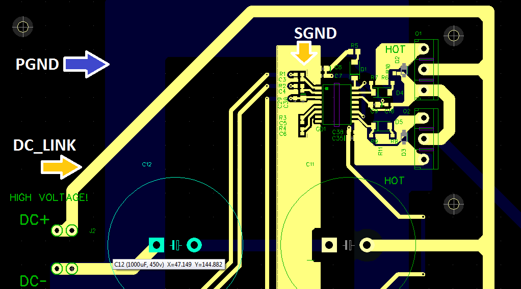
Layout with DC-Link
IGBT Capacitance
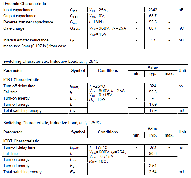
As per the input capacitance and gate charge, the selected value of Cboot is well above the recommended value. I'm unable to quantify the cause of the high side failure. The distortion occurs at the driver stage and is reflected in the microcontroller board. I have routed PGND and SGND separately and shorted them at only one point (not shown in the layout above)
So, what is causing the problem? How to solve the issues? HAAAALP ME