


Hi team
my customer has a design requirement via TPS3700
The input voltage (Vmon) is used to supply power to MCU, normally around 3.3V, so they need to design a voltage monitoring and protection circuit now:
1. When the input voltage (Vmon) is 3.6V ~ 4.7V, a falling edge signal is output to reset the MCU reset pin (RST).
2. When the input voltage (Vmon) is greater than 4.7V, a low-level signal is output to turn off the DCDC supplying power to the chip.
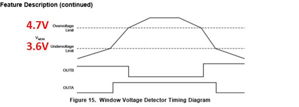
In this design, I used the resistance calculation software on the page of tps3700. After I input the required voltage, I get the resistance(R1,R2,R3) of the peripheral circuit.


Then I use Tina to build the simulation circuit. Through simulation, it is found that the result is not consistent with the theory. OUTA does not have high-level jump when Vmon is greater than 3.6V.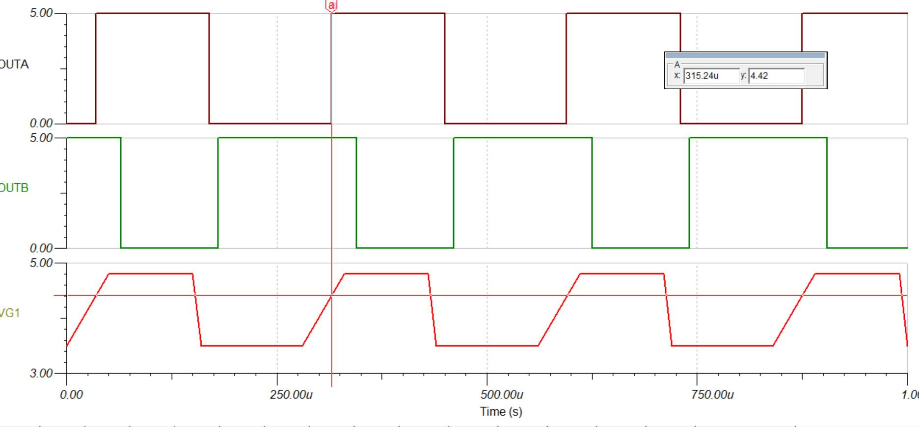

1. Could you please help me analysis that result ?
2. Could you please give me a design based on my customer ' s requirement and help me calculate the R1,R2,R3 and Rp value?
Best regards
Jean Liao
jean-liao@ti.com