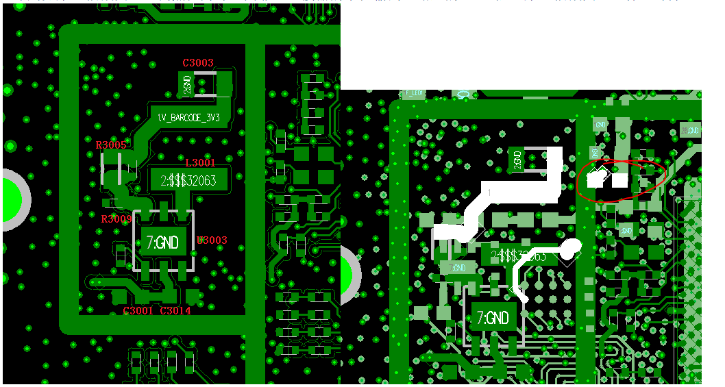
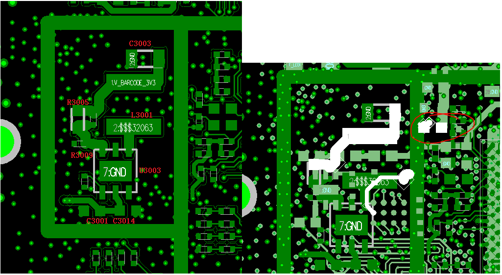
This thread has been locked.

If you have a related question, please click the "Ask a related question" button in the top right corner. The newly created question will be automatically linked to this question.

TPS62250: There's an instant pressure drop

Part Number: TPS62250

Hi:

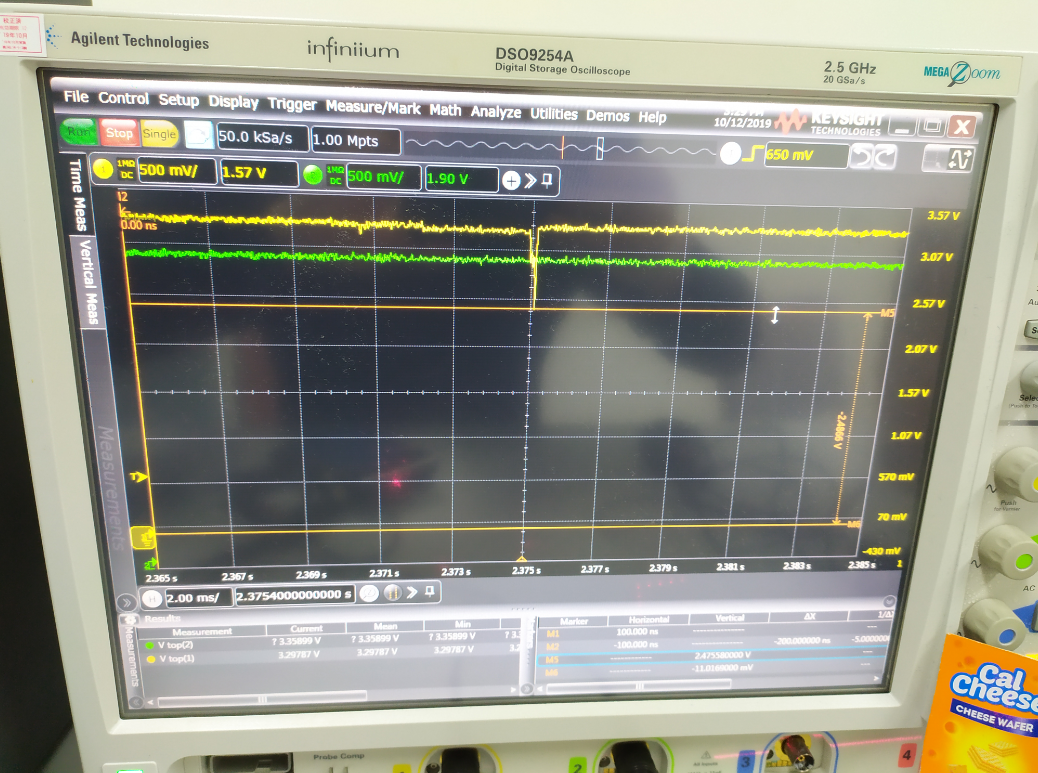
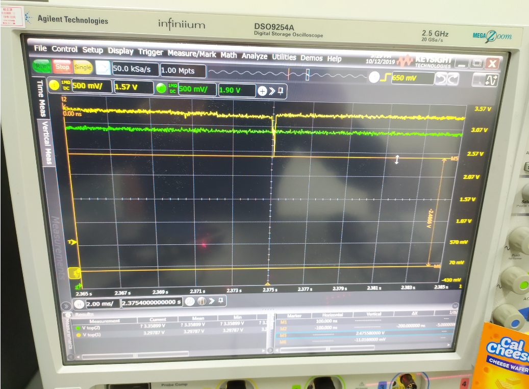
I used TI TPS62250 IC for dc-dc voltage conversion, with input voltage of 3.5-4.35v (battery voltage) and output voltage of 3.3v.At present, the maximum instantaneous load demand of the backend is around 900mA. When I measured it, I found that there would be an instantaneous pressure drop.

Application scenarios:

Because the backend is a scan terminal module, there may be an instantaneous peak value of 900mA when scanning code at a distance, and there is a probability of voltage drop.

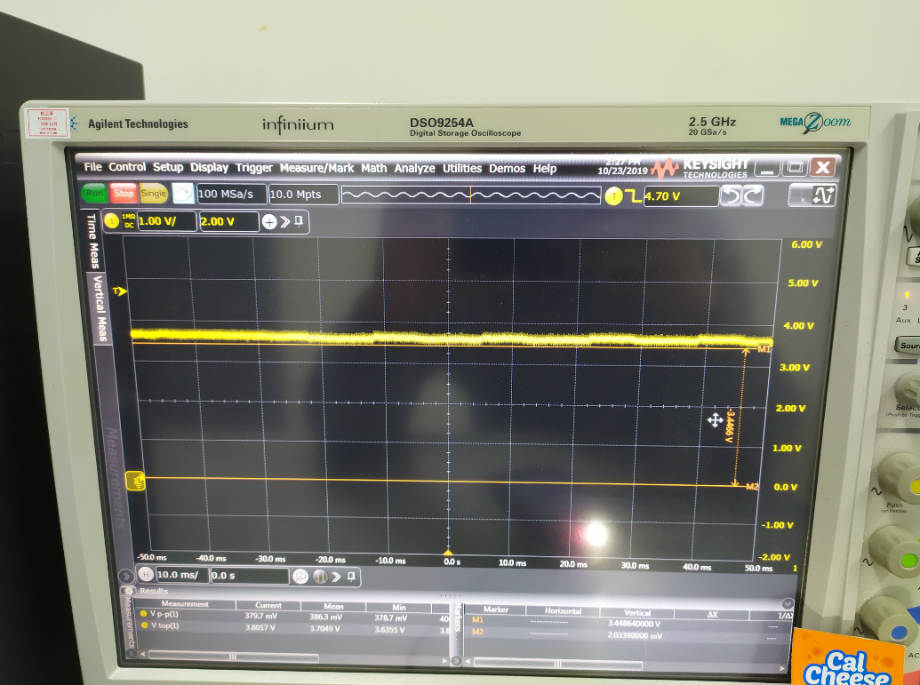
What I did:Increase the output capacitance a little(22uA),There will be improvement, but the voltage drop will still be there, but the voltage drop will be a little bit smaller.Also please help to give some advice, thank you.

The schematic diagram is as follows:

The waveform is as follows:

  • Hi,

    Schematic looks reasonable but could you provide more detail about the cap, inductor and battery used in the schematic?

    Voltage drop occurs when the 900mA load is applied to the device. So, could you provide the plot of ILoad with input and output voltage? 

    Best regards,

    Tanvee

  • Hi Tanvee:

    The following is the reply to the question, please help guide, thank you.

    1.In the schematic diagram, the model of capacitor & inductor.

    2.Input and output waveforms

    (1)Input waveform

    (2)Output waveform

  • Hi,

    Thanks for the information.

    In the second waveform, could you specify which one is output voltage and the point where the output voltage is dropping is it the point where are you applying the load? Could you share which point are you measuring the output voltage and could you also share the layout? If the information is confidential then I would suggest it to share it through the mail.

    Best regards,

    Tanvee

  • Hi Tanvee

    1.The yellow waveform line is the output voltage (3.3v), the sharp one is the drop point (2.57v), and the green waveform need not be seen。

    2.The output voltage of the second diagram is measured with a constant load, but it is impossible to determine which is at the maximum load point, because the load varies with the power of the scan code.Layout as shown in the first screenshot, the measurement point position on the other side of the string near the connector is in the 0R resistance of the heavy output circuit (red marked part in the second screenshot).

  • Hi,

    It seems when you scan the code, the max load is applied to the device with a very fast slew rate and making a drop in output voltage.  Thts the main reason I want to see the load waveform on the same conditions. Could you able to measure it in the output voltage and load at the same condition and try to measure the output voltage on the output capacitor (C3003)

    Best regards,

    Tanvee

  • Hi,

    I didn't heard back from you. I am closing the thread if you have further questions feel free to contact through thread or mail. 

    Best regards,

    Tanvee