This thread has been locked.

If you have a related question, please click the "Ask a related question" button in the top right corner. The newly created question will be automatically linked to this question.

UCC27517A-Q1: Reverse Battery Capability

Part Number: UCC27517A-Q1

Dear, Sir.

My customer is considering to apply UCC27517A-Q1 for their automotive system.

Now, they are cheking the capability against reverse battery.

Before, they faced a trouble on other supplier's product such as;

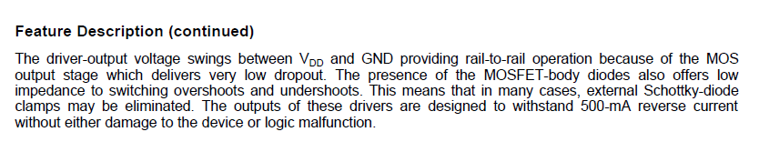
There was the current flow from OUT pin to external FET gate under reverse battery condition.

The FET turned on due to abobe current flow(maybe there was a path reverse battery/GND - OUT - GATE).

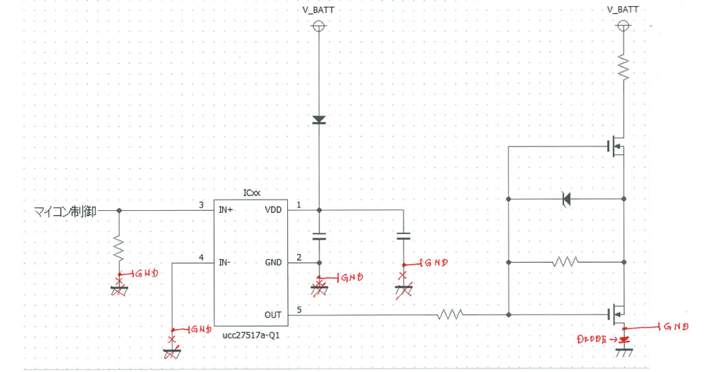
They will put the external transistor on VDD pin, so VDD will be off during reverse battery condition.

Please give your advice on following;

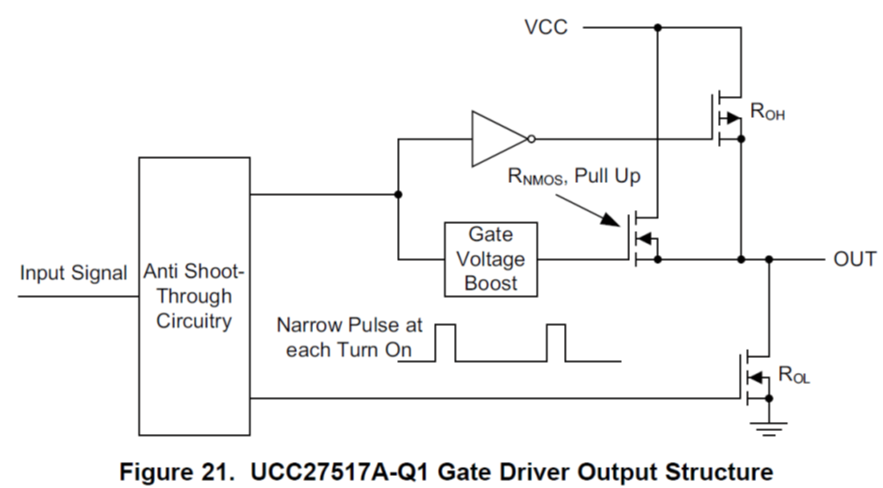
1. Does UCC27517A-Q1 have the weakness or concern against reverse battery condition similar as the example

    of OUT pin current flow?

2. If you had a concern, however had a solution against it, Please let us know.

3. I worry about the body diode on the external FET. It will be forwarded. Do you have any idea to protect that?

Best Regards,

H. Sakai

  • Hello Sakai-san,

    Thanks for your help promoting our drivers.

    To the best of my knowledge, we have not encountered any specific issue with false turn-on of the FETs caused by reverse current from GND. 

    Can you please elaborate on reverse battery conditions? How is the battery connected to FET and driver IC beside sharing the same GND (I assume). What voltage/current levels do GND reach under reverse battery conditions? 

    To accurately address question 3, I would need to take a look at the schematic.

    I'd be happy to review customer schematic/layout (if you can drop me an email or post here if not NDA restricted!) to ensure best performance from UCC27517A-Q1. 

    Regards,

    -Mamadou

  • Dear Mamadou-san. 

    Thank you so much for your kindly reply. 

    Below is the rough schematic for UCC27517A-Q1. The component values are not decided. 

    Under reverse battery condition, V_BATT will be connected to - of battery & GND will be 

    connected to + of battery. The battery voltage will be typ. 12V, + to -. 

    The customer is concerning if ROL FET has the body diode, the current flow to OUT pin would be

    happened. 

    Could you please check and give your advice for us. 

    Best Regards, 

    H. Sakai

  • Dear Mamadou-san. 

    Regarding my previous question about the body diode on ROL. 

    There will be the body diode on ROL according the datasheet description. 

    I also checked the simulation model. I could see the leakage due to the body diode. 

    So, I tried to consider the solution. 

    1. Put the diode between the bottom side external FET and GND. 

    2. All IC's GND will be connected to the Anode of diode. 

       IC's GND voltage will be elevated to VF of the diode. 

    Is it no problem taking this kind of usage?

    Please give your advice. 

    Best Regards, 

    H. Sakai

  • Hello Sakai-san,

    Thanks for the additional information. 

    You're correct the N-ch FET does have a body diode which generally helps in undershoot conditions as mentioned in the d/s.

    You mentioned that you've seen the leakage during simulation, can you please share simulation files/results.

    From the driver's perspective, the diode between IC and GND seems reasonable to address customer previous issues but I would caution that the IN+ signal will then be referenced to a slightly lower potential as IN+ will be at 0V while driver IC is at ~0.7V. I suggest to account for the IN+ signal amplitude and the driver's VIH and VIL thresholds. You might consider a discrete pnp level-shifter between IN+ signal and driver's IN+ pin to overcome this difference in potential.

    Please let us know if you have additional questions or press the green button if this addresses your concerns.

    Regards,

    -Mamadou