This thread has been locked.

If you have a related question, please click the "Ask a related question" button in the top right corner. The newly created question will be automatically linked to this question.

TPS548A20: No output, possible design error?

Part Number: TPS548A20

Hi there, 

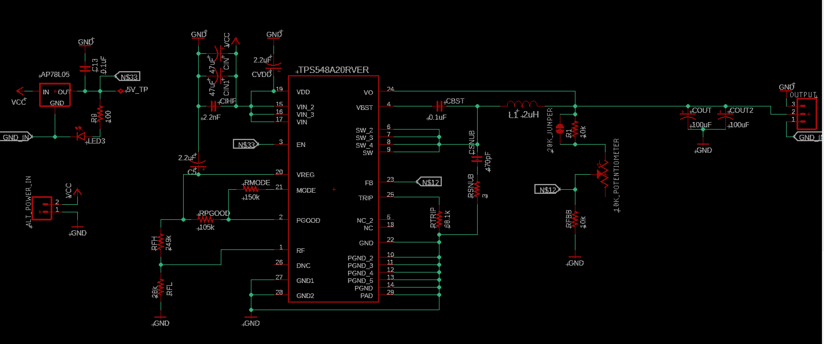
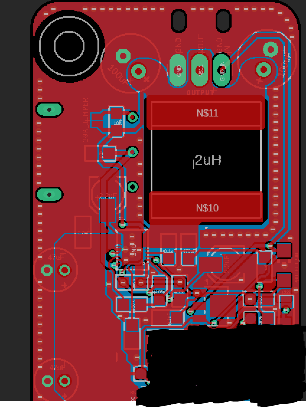
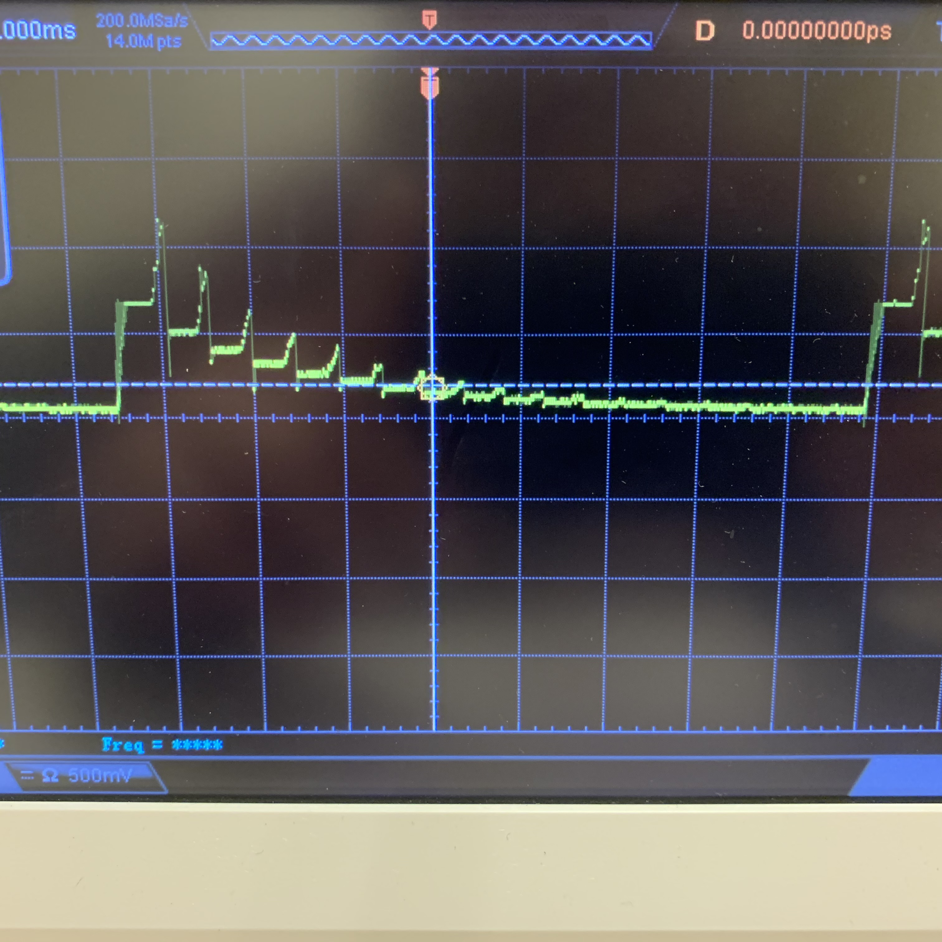
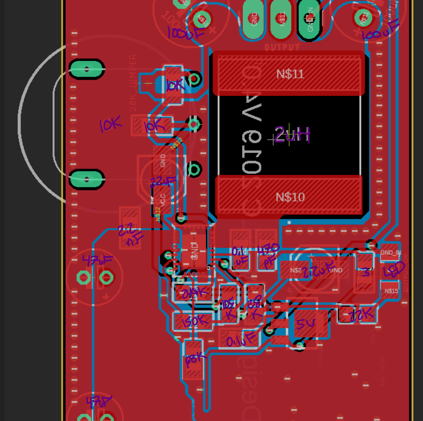
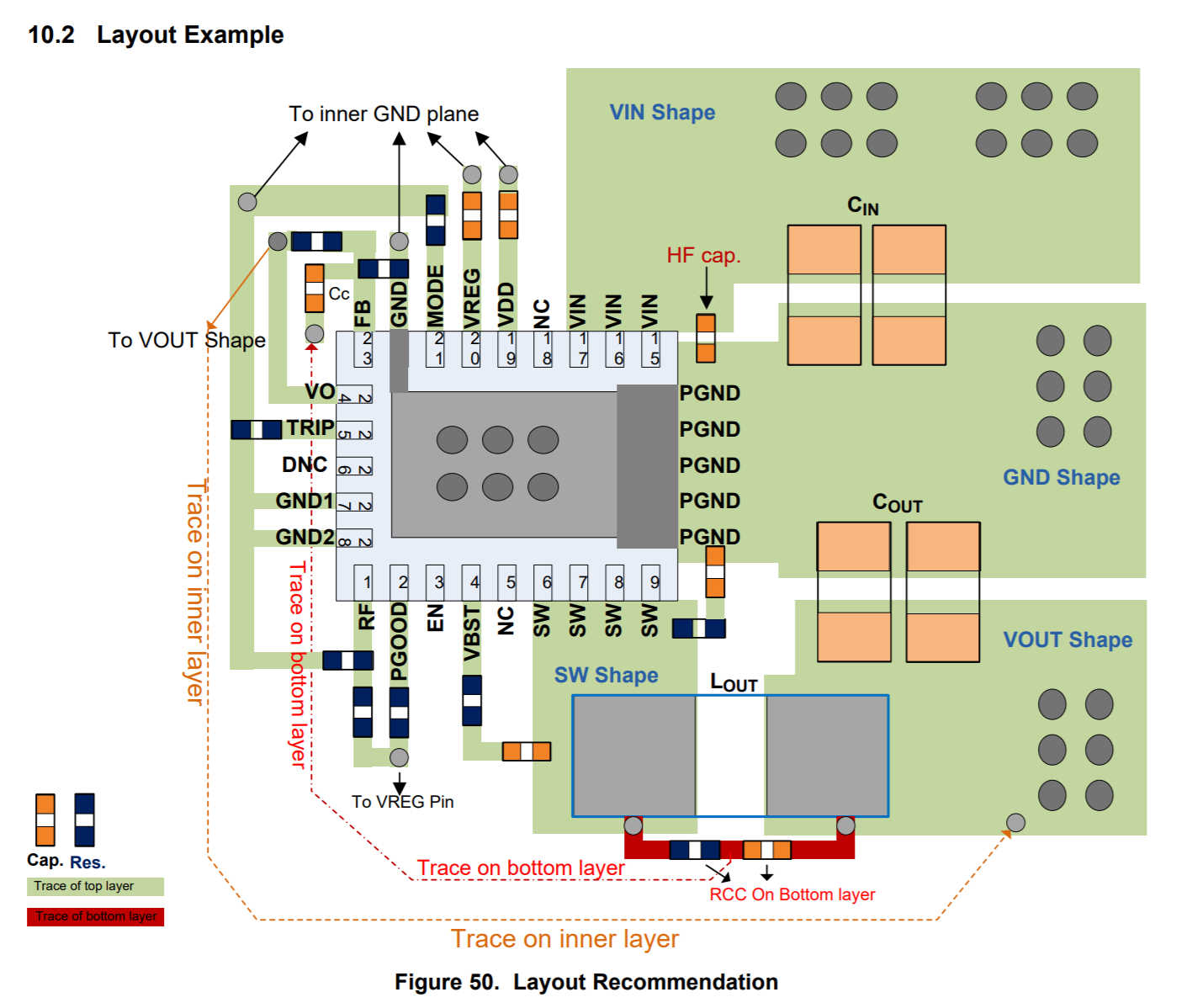
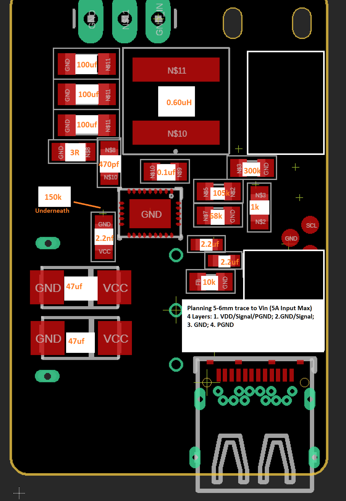
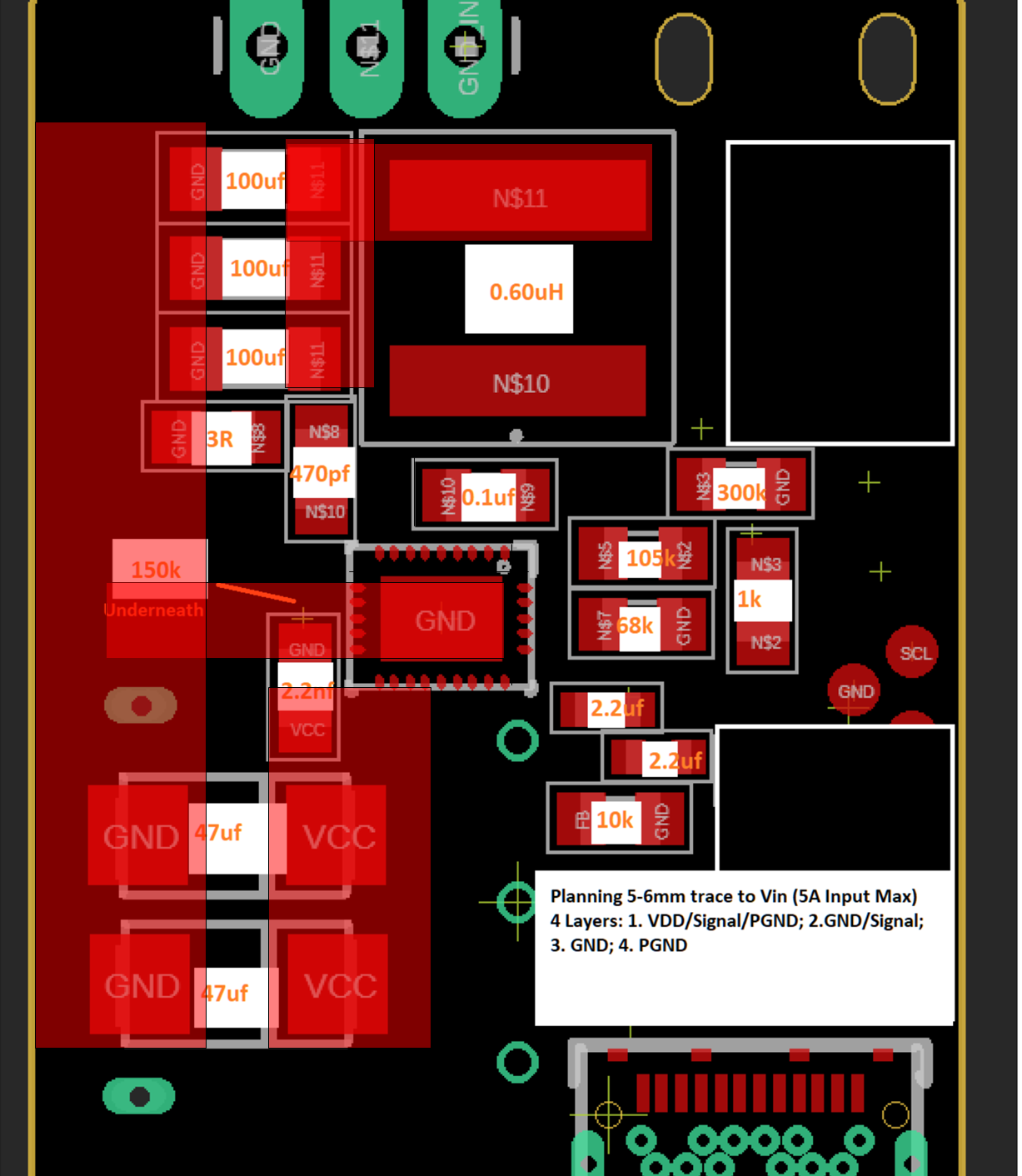
I'm running into some issues with receiving the correct output voltage. I used the Webench tool to design a 1.2-1.8V @13-15A output goal. The source voltage is 20V. I've set the frequency to 300kHz using a 68k resistor. The inductor is 2uH. When I power it up with 19V I received an output of 0.1V and its current consumption is 0.005. I'm certain its properly grounded, it was attached via reflow. I've attached a schematic, board design, and a waveform from the output. 

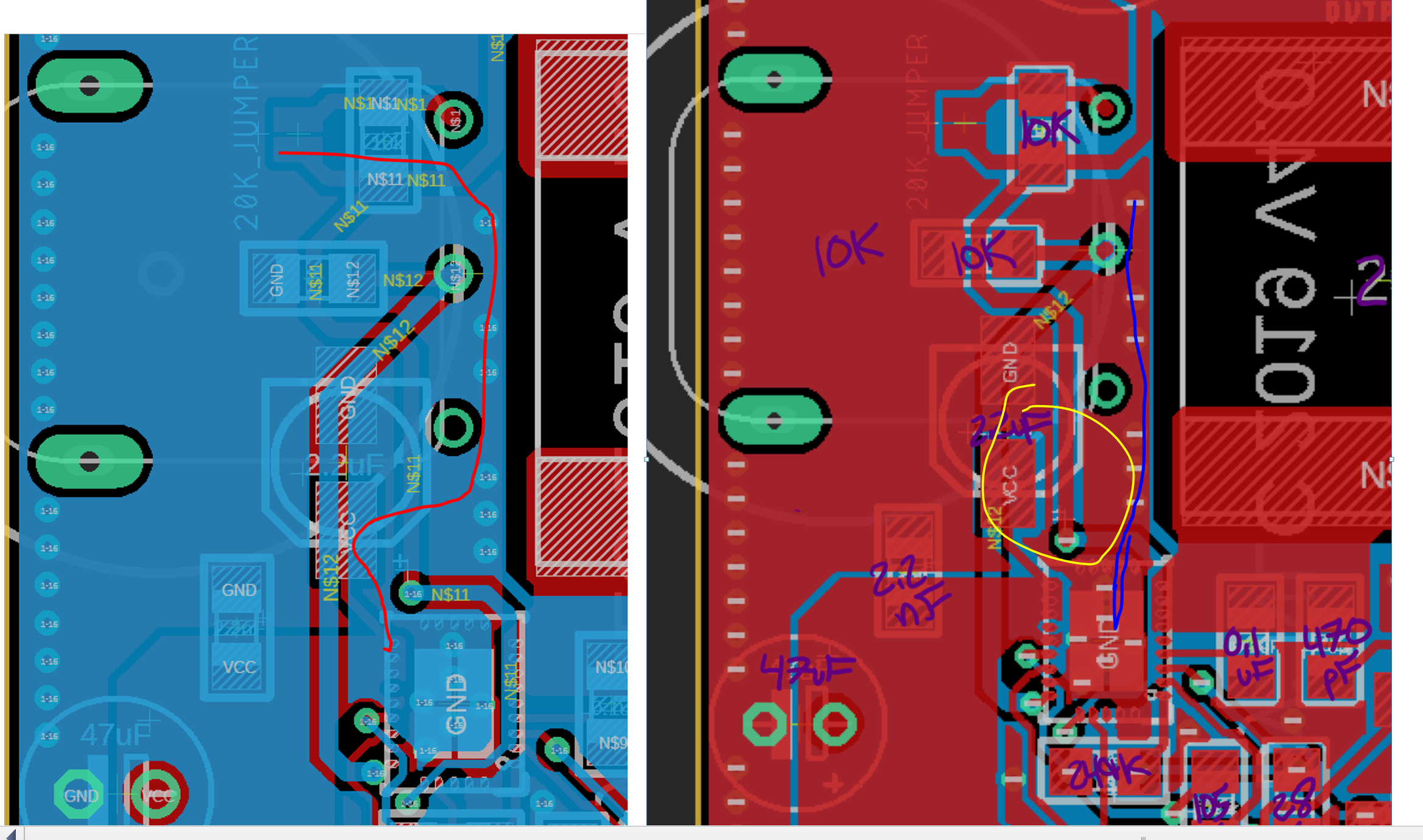
Correction: 28K & 249K for 300khz.

  • Hi,

       Can you please create a link to the WEBENCH design and share here? It will help with the debug.

    Regards,

    Gerold

  • I think the power ground is not big enough and the input capacitors need to be placed differently. 

    What is the width of the ground copper from the pad under the device to the input voltage supply ground.

    Look at the layout in figure 50 of the TPS548A20 datasheet, the copper power is wide and not cut with other traces and there are lots of vias.

    When you board is operating, check the input voltage on the device pins.  

    Try getting the capacitor grounds closer to the copper pour of the device ground.

    Regards,

    David

  • Hi Nick,

       To add to Dave's comment, please ensure that the GND is used for analog signals and PGND is used for the high current return as power ground. GND should be connected to the thermal pad using a small trace.  Refer to Figure 50 in the datasheet for layout guidelines.

    Also, are the input and output capacitors electrolytic or ceramic. If electrolytic only, please add ceramic to minimize the ESR.If ceramic is used, ensure that you have sufficient capacitance considering the DC bias derating of the capacitors.

    regards,

    Gerold

  • Hi David & Gerold, 

    I took a picture of the GND plane on the bottom of the board to give a better perspective of the overall GND plane. I'm going to scrape some of the soldermask off the top of the GND plane connected to the bottom of the IC and place a wire to increase the GND connection. 

    I have the thermal GND plane under the IC connected to the same GND as the PGND, could this cause a significant issue? I have vias under the IC connecting it to the GND plane on the bottom of the board as well. 

    My 47uf capacitors are low ESR electrolytic, 2.2nf is ceramic, and 2.2uf is surface mount electrolytic. 

    The vin trace to the IC is approximately 1.7mm but narrows down to 1mm as it connects to the first 3 vin pins. 

    Thank you,

    Nick

  • I  think the input ground and vin loops need to be shorter and wider.

    The input capacitors need to be very close to the VIN and PGND pins and have the most direct connection to 

    minimize parasitic resistance and inductance.

    The blue copper pour has a narrow path to the larger ground plane.

    The red copper pour connects to the blue ground plane through vias but still has the long path to the larger ground plane.

    The red copper pour connects to the larger red ground plane through a very narrow trace circle in yellow.  

    Connecting the PGND to the thermal GND should not cause a problem,

    but it is not recommended to circulate significant current under the device.

    Below is an example of a TPS548A20 layout,  the high current loop is on the right and the quiet ground connect to the pad under device. 

    The high current loop is short to minimize parasitics and the input capacitors are close to the vin and pgnd to minimize transients on the supply so that the device will operate well. 

    As best as you can mimic the input and pgnd on your board and check the input voltage at the VIN and PGND using  the tip and barrel technique.. 

    David

  • Gentlemen, I've put together another board layout. This time the board will be 4 layers and I will be sure to place a heavy amount of vias for Vin and PGND. I've attached an initial placement of the components focusing on the placement to be as similar to Figure 50. Your feedback would be appreciated. Additionally, I've changed my frequency from 300kHz to 1Mhz for sizing reasons. All capacitors will be ceramic except the two input 47uf caps which I'm planning on being tantalum. I'm planning on a 5mm width Vin trace and separate GND and PGND traces. Your thoughts are appreciated. 

    Best,

    Nick

  • I think this layout will work better for you.   I sketched where the pours could be.   I would consider changing the size of the boot capacitor to a smaller one and widening the sw trace from the pin to the inductor.   Consider adding a resistor in series with the boot cap to reduce sw node ringing.    Be cautious when pouring the ground plane with the automated software features, with your layout you should be able to have a quiet ground for the fb and mode components.   Maybe use a different net name or have a 0 ohm resistor to separate the power and analog grounds.

    Best Regards,

    Davdi

  • Thank you David,

    Just to confirm you are talking about reducing the size of the boot cap from 1206 to say a 0603? Would a 0-ohm resistor work in series with the boot cap? I'll be creating the GND pours by hand. I plan on having a layer dedicated to the isolated GND which I'm not sure where to connect at the moment, would it be optimal to connect it to the GND of the input, the GND at the output, both, or possible only at pin 22? 

    Thanks,

    Nick

  • Nick

    Just to confirm you are talking about reducing the size of the boot cap from 1206 to say a 0603? Would a 0-ohm resistor work in series with the boot cap?  Yes,  0603 capacitor and 0 ohm in series.    If there is too much ringing on the SW pin, the 0 ohm can be changed to 1ohm to reduce the ringing

    I'll be creating the GND pours by hand. I plan on having a layer dedicated to the isolated GND which I'm not sure where to connect at the moment, would it be optimal to connect it to the GND of the input, the GND at the output, both, or possible only at pin 22? 

    The quiet ground should connect to pin 22 and you need to use only part of the top layer (see the top layer of the see figure 50 in datasheet) to connect the FB resistors, Rtrip, etc. The power ground should be your separate plane, connect with many vias under the device and the the input and output capacitors ground.