This thread has been locked.

If you have a related question, please click the "Ask a related question" button in the top right corner. The newly created question will be automatically linked to this question.

TPS50601A-SP: thermal performance and operating maximums

Part Number: TPS50601A-SP

Team, 

Two questions: 

1) Can you provide the maximum operating supply current for TPS50601A-SP? as well as the maximum output voltage. A note from the manufacturer on these two items is needed for WCA documentation for an end customer. 

I realize that it is a 7V in 6A out device, which could provide the theoretical max input current and output voltage of a DC/DC buck reg. however a calculation is not sufficient for the end customer and a spec is being asked for. 

in addition:

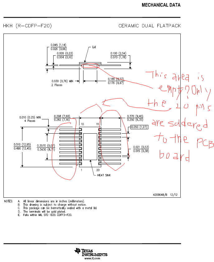
2) When the 20 pins of the TPS50601A-SP device is soldered to the PCB board, I believe the bottom case of the 50601A-SP device is floating in the air, and the area which I circled is empty , and when there is 1W loss in the TPS50601A-SP device itself, the worst case temperature rise of the internal junction of the TPS50601A-SP device will only have 0.514 deg. C temperature rise above the ambient temperature ? i.e. this is the absolute worst case temp rise per watt the device will encounter. and this can be used in the WCA effort to bound the temp rise. 


  • [CY] From my perspective, a WCA requires a complete converter design be analyzed. Because of the versatility of the TPS50601A-SP there are numerous (if not infinite) implementations possible. With that said, the responses to the questions are very generic since no details of a design are provided.

    Q1:  Can you provide the maximum operating supply current for TPS50601A-SP?

    The datasheet specs Vin at a maximum of 10 mA during operation.  The max current for PVIN  depends on the output current/efficiency/output voltage/input voltage for the system, all determined by the designer.

    Q2:    ...as well as the maximum output voltage?

    The device supports a maximum duty cycle of 100%, thus, the maximum possible output voltage is the input voltage times the efficiency.  A more meaningful analysis would determine the max output voltage given a specific duty cycle.

    Q3:  However a calculation is not sufficient for the end customer and a spec is being asked for. 

    [CY]  A spec will not be possible as characteristics of external L and Cs, outside the control of our processes, also influence worst case.

    Q4: When the 20 pins of the TPS50601A-SP device is soldered to the PCB board, I believe the bottom case of the 50601A-SP device is floating in the air, and the area which I circled is empty , and when there is 1W loss in the TPS50601A-SP device itself, the worst case temperature rise of the internal junction of the TPS50601A-SP device will only have 0.514 deg. C temperature rise above the ambient temperature ? i.e. this is the absolute worst case temp rise per watt the device will encounter. and this can be used in the WCA effort to bound the temp rise. 

    [CY] Firstly, the device should not be floating in air.  The circled part of the picture you provided is the heat slug of the package and should be mounted to a sufficient heat sinking mass on the PCB.  Page 4 of the SMD for this device defines such a heat sink in the test board conditions.

    Test board conditions:

    a. 2.5 inches x 2.5 inches, four layers, thickness: 0.062 inch.

    b. Two ounces copper traces located on the top of the PCB.

    c. Two ounces copper ground planes on the two internal layers and bottom layer.

    d. Four 0.010 inch thermal vias located under the device package.

    Regards,

    Christian