This thread has been locked.

If you have a related question, please click the "Ask a related question" button in the top right corner. The newly created question will be automatically linked to this question.

TPS92641: Application of TPS92641

Part Number: TPS92641

Hi team,

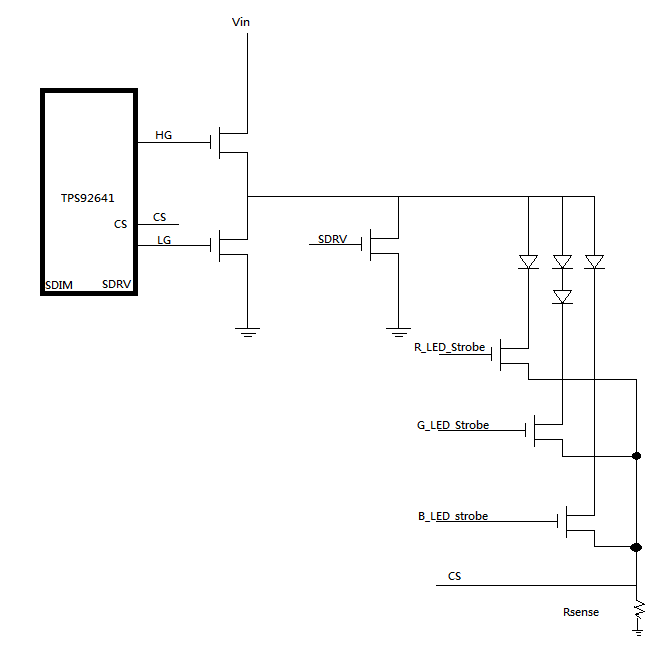
Customer would like to consult the application TPS92641 as below schematic.

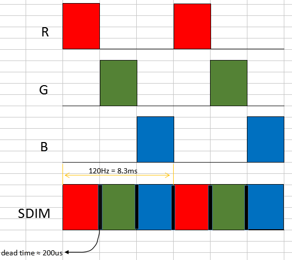
There will be three connected LED which is controlled by strobe signal with mosfet and the strobe signal will not been overlapped.

  • Does the structure make sense for you? Would you have any concern about it?
  • Because the Vfb signal is different for different LED, whether there will be a voltage spike since transition?

Thank for your help.

  • Hello,

    This can be made to work provided the timing is done correct with R, G, B and SDRV.  It will also depend on the pulse widths and PWM frequency.  There will be current overshoot if the load dynamically changes, it depends on what is acceptable.

    Is the idea to use the SDRV to shunt when switching R, G and B?  What will the output voltages be for R, G and B?  What pulse widths and duty cycles is this going to use?  What is the input voltage, output current?

    "Because the Vfb signal is different for different LED, whether there will be a voltage spike since transition?"  Since this is an LED driver the concern is current spike and yes, if the output voltage changes instantaneously it will have overshoot and undershoot.  The amount will depend on many factors.  To avoid this would be to go to a hysteretic LED driver.

    Best Regards,

  • Hello,

    I haven’t heard back from you, I’m assuming you were able to resolve your issue.
    If not, just post a reply below (or create a new thread if the thread has locked due to time-out)

    Best Regards,

  • Hi Irwin,

    Sorry for the late. Please refer the feedback as below.

    Is the idea to use the SDRV to shunt when switching R, G and B? 

    pic1 is our control signal, I think that SDRV should work at dead time(switch off) and avoid current spike(overshoot or undershoot)

    But I dont know whether another risk or not on this design. 

    What will the output voltages be for R, G and B?

    R = 3.2V

    G(including Pumping LED blue) = 7.6V

    B = 3.6V

    What pulse widths and duty cycles is this going to use?

    pic1 as below

    What is the input voltage, output current?

    input Voltage = 19V

    output current = 8A

  • Hello,

    Using SDRV to shunt for 200 uS will not prevent the overshoot/undershoot.  The TPS92641 holds the compensation voltage constant when the Shunt FET is on.  If the output voltage changes the compensation has to change so there will be overshoot or undershoot.  The overshoot will happen when the load is running at 7.6V, shunted then opened with a lower voltage string which would be the blue in the above sequence.  Red and Blue are fairly close in forward voltage so that may be fine.

    This is a fairly slow switching sequence, perhaps a capacitor across the LEDs and lower compensation capacitor value may make this acceptable for your application.  Is there a limit on overshoot and undershoot on this design?

    Best Regards,