This thread has been locked.

If you have a related question, please click the "Ask a related question" button in the top right corner. The newly created question will be automatically linked to this question.

Impedance Balancing

My apologies if this isn't the most appropriate forum to ask this question, but I have found the response from users on this form to be extremely helpful in the past with my electrical questions.

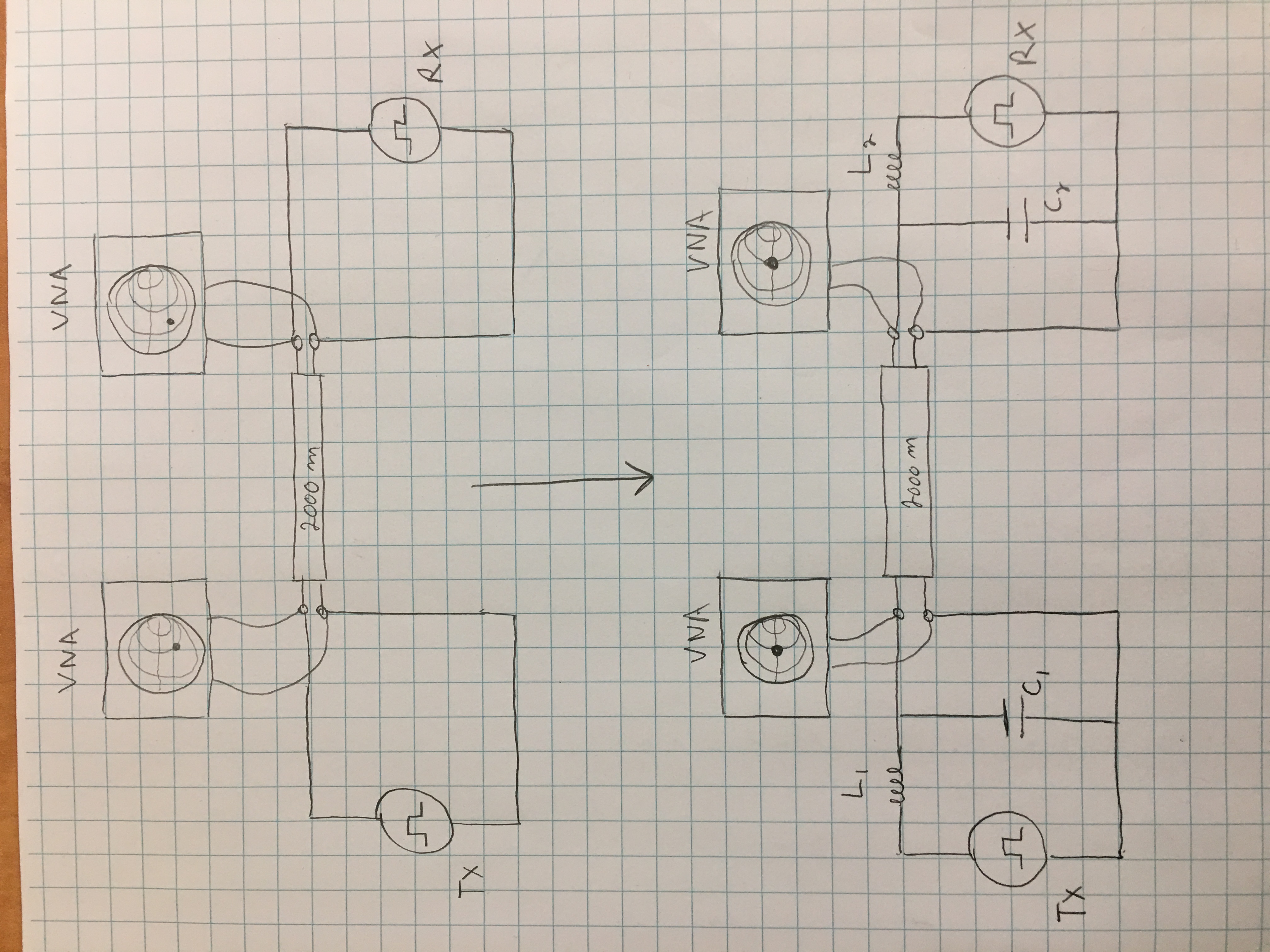
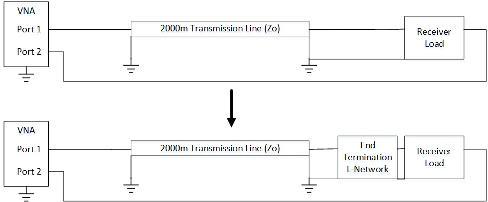
I am new to impedance balancing so bear with me. I have a transmitter and receiver with 2000 meters of electrical cable connecting the two. The signal I am transmitting is a 3.3 volt digital signal. I am trying to impedance balance this network and a bit confused where to hook up my VNA.  I drew a diagram below, is this correct?  If I understand it, my VNA connects to the transmitter circuit while it is connected to the 2000 m transmission cable, which is then connected to the receiving circuit. Using my VNA and a Smith Chart, I will impedance balance the TX circuit with some "L" network including a certain value inductor and capacitor.  After that is balanced on the VNA, I connect my VNA at the receiving end and do the same type of impedance balance.

Does this make sense or am I going about this wrong?  Thanks for any input anyone has.

  • Hi Dustin,

    Thanks for your question.  We should be able to give you some guidance on this.  We were a little tied up today and it's a complex topic, though, so we will get back to you early next week with a more detailed response.

    Regards,

    Max

  • Hello Dustin,

    Thank you for your question and I apologize for the delay in getting a full response to your question posted.  I will preface this post and claim while I would not consider myself an expert in this field, I have a basic working knowledge of the principles and methods.  Hopefully I have understood your question correctly and put together an informative and comprehensive overview of the process you will find helpful.  I have not gotten into any of the calculations and instead tried to keep this pretty high level.  If you have any more questions I can certainly try to address them.

    The high level approach you suggested is pretty much correct but I will comment on a few things.

    In your diagram you show a VNA and a TX Data transmitter source. During this process, the VNA becomes the transmitter source and simultaneously transmits a sine wave of a particular frequency and monitors the line for both the transmitted signal, and any reflected signals which it uses in its calculations. You can typically set the VNA to use a particular frequency, or to sweep a frequency range. When you are trying to match impedance, you will need to use a single frequency.

    Also, of importance is that you will need to place the VNA on the other side of any of your L-Networks and not as shown in your figure. The ports of the VNA need to see the signal “through” the components and not at the end of the transmission line before the signal as passed through the matching network components. These components are added to the Load and therefore the VNA must be connected at the far end of the network.

    Also, I’ll discuss more later in the post, but typically you will only place a matching network on the Load side of the transmission line near the receiver and you do not need to match the source impedance to the characteristic impedance of the transmission line if the load impedance is properly match to prevent reflections traveling back down the transmission line to the source. 

    The following two diagrams would be where I would make the connections. First, connect one port of the VNA to the transmission line and the other to the far end of the “load” which will include the receiver. Then, use the Smith chart to calculate the proper L-Network component values and add them into the system and tune the system until the Load impedance seen by the transmitter equal the characteristic impedance of the transmission line.

    It definitely needs to be pointed out and understood that the “Impedance” is frequency dependent and will vary with the frequency. Even though you are transmitting a “digital” signal, you are really sending a complex analog waveform down the transmission line and you should think about it from an “analog” perspective such that your waveform is the product of numerous harmonics of a fundamental frequency sine wave which come together to create a more “square” waveform that will represent a digital “bit.” The fundamental frequency is a product of the signal’s rise time and will vary with different transmitters.

    The Fundamental Bandwidth Frequency:

    –       A pulse of energy occurs when a signal switches current and the majority of that energy comes from a signal at a frequency referred to as the “Fundamental Bandwidth” or the “First Harmonic Frequency”

    –       The Fundamental Frequency will increase as the switching time increases.

    –       The remaining energy in a pulse comes from harmonics of the Fundamental Bandwidth Frequency.

    –       The Fundamental Bandwidth Frequency and its Third-Harmonic should be used in calculations and not the signal’s clock or data rate for many types of calculations.

    –       To Calculate: tr=2.2τ = 2.2RC = (2.2)/(2πFbw) = 0.35/Fbw                 

                                           Fbw= 0.35/tr           (where tr is in nS and Fbw is in Ghz)

    –       For Impedance Matching, we care about the reflection coefficient between the transmitted and reflected power. The spectral power density of a digital signal will display nulls at multiples of the clock/data rate with a -20 dB/decade slope from Fclock (or data rate) up to the “Knee Frequency.” Beyond the Fknee frequency, the spectrum rolls off much faster than 20 dB/decade and the spectral amplitude is down by more than half of the natural rolloff. This knee frequency for a digital signal is also related to the rise/fall time of the digital transition edges.

    –       To Calculate: Fknee = 0.5/Tr

    Where Fknee = frequency below which most energy in digital pulses concentrated

    and Tr = pulse or digital edge’s rise time

    –       The Fknee will be higher for shorter rise times, and lower for longer rise times. The spectral content below Fknee will be responsible for most time domain characteristics and any circuit with a flat frequency response up to and including Fknee will pass a digital signal relatively undistorted. Likewise, there will be little effect from the processing of frequency content above the Fknee frequency.

    –       For purposes of impedance matching we should use concern ourselves at frequencies between Fclock (or the data rate) and the Fknee.  

    I would suggest you evaluate your system around the first and third harmonic frequencies as well as the Fknee frequency determined by your transmitter’s rise time, to evaluate the impedance matching networks of your system. Any harmonic frequency content that is not properly matched will be reflected back to some extent and result in a Voltage Standing Wave, or Standing Wave, and is commonly evaluated as a ratio (VSWR or SWR) and is a measure of the load impedance relative to the characteristic impedance of the transmission line which together determine the reflection coefficient. The SWR is also defined as the ratio of the partial standing wave's amplitude at an antinode (maximum) to the amplitude at a node (minimum) along the transmission line which we want to minimize by matching the load and characteristic impedances. The amount of reflected energy will add or subtract with the source signal at regular intervals creating a standing wave on the bus. A larger SWR value will mean that there is more reflected energy on the transmission line and the impedance is not optimally matched. Since we can only match for a particular frequency, the power from harmonic frequencies in a digital signal will prevent a perfect SWR and we need to optimize for the frequency responsible for the majority of the energy.

    There are three different impedance values that need to be considered in a system like this. There is the Source Impedance ZS, the load impedance ZL, and the transmission line’s characteristic impedance ZO.

    If you were to connect the Load directly to the source without going through the transmission line, the impedance of the Load that the Source sees will be different than the impedance of the Load seen by the source looking “through the transmission line.” The VSWR seen by the source is Constant, but the actual Impedance changes. This means that different impedance values will result in the same VSWR, or amount of reflected energy.

    This is because adding or subtracting length to the transmission line will rotate you around the Smith Chart and change the complex impedance. Each rotation around the chart will represent ½ of the frequency wavelength (λ/2) and each half rotation will result in a ¼ wavelength (λ/4). The ZINPUT will equal ZLOAD when the length is a multiple of λ/2, regardless of the ZO or ZLOAD. The transmission line that is exactly a multiple of λ/4 length also has interesting properties in that it will appear to the source as an Open if it is shorted, and it will appear as a Short if it is Open due to the way the waveform reflections will interact with the source waveform. Therefore the exact length of the transmission line will determine where the complex impedance will be on the Smith Chart and what series and shunt L/C components will be required to match the impedance. If the complex impedance was plotted in the following Smith Chart such that is was on the Constant VSWR line, changing the transmission line length would cause that impedance to rotate around that circle through the Smith Chart.  If you have already created a matching L-Network, this would cause your "matched" network to no longer be matched and it must be re-calculated.

    There are three standard methods for ensuring a flat frequency response:

    1. End Termination: Adding series and parallel (shunt) inductor and capacitor elements to the load to match the impedance seen by the source equal to the characteristic impedance of the transmission line.
    2. Series (source) termination: Adding series and parallel (shunt) inductor and capacitor elements to the source to make the source impedance equal to the characteristic impedance of the transmission line. Note, this will allow for all reflected energy from the load to travel back towards the source before it is terminated.
    3. Shorten the line to make it “electrically short” and not behave as a transmission line. This is not an option for you with a 2000m cable unless your frequency content was extremely low.

    In your diagram, you show a TX side and a RX side and if data will flow in a single direction, you typically only need to implement one type of termination method (end or series termination) but not both types. End termination is the most common allowing the source to transmit the full spectral content of the signal into the transmission line and adjust the load impedance to match the characteristic impedance and eliminate any reflections that could be destructive to the signal.

    However, if the data is bi-directional, both sides of the transmission line may need to be addressed and both the source and load impedance’s will need to be matched to the characteristic impedance. One thing you will need to remember is that the series and parallel (shunt) inductor and capacitor elements that are added to the network will act as some form of filter and could cause other problems in successfully transmitting the data across the network. Reducing the number of filters and also carefully selecting the right component values will be critical to the overall success.

    Using a series Inductor will be more of a “Low Pass” filter, while using a series capacitor will be more of a “High Pass” filter.

    I believe that if you need to create a matching L-Network on both sides of the transmission line, you will need to do one side at a time, and then start an iterative process where you go back to evaluate the first network given the load changes you made to the second network since the system has changed since the first calculations were made. Since both sides will be the source and the load, this may take some time to get set correctly.

    After you have Normalized and plotted your complex load impedance as seen by the source through the transmission line on a Smith Chart, or viewed it on the VNA, your load will fall into one of several areas that may change the type of L-Network you choose to use. If your load falls into one of the un-shaded regions of the following figures, the corresponding two component network can be used to match the impedance to the normalized system impedance which is at the center of the Smith Chart.

    Adding Inductance causes you to “rise” upwards on the chart, while adding capacitance will cause you to “fall” downwards on the chart. Once again, the type of elements and network you chose may also need to be a consideration of other system goals and requirements such as Low/High Pass filtering, realistic values of components, etc. More complex networks can be created by adding more than 2 elements .

    You will typically add a series or parallel (shunt) element to move you to one of the Resistance or Admittance circles and then add the other component to move you to the center of the chart and the normalized system impedance which is typically 50Ω, 75Ω, or 100Ω, etc. depending on your transmission line cable.

    Here is an example of how a Series C + Shunt L network would move the impedance on the Smith Chart.

    I hope this was informative and addresses your question, and also not so extreme that it was too much information to cause more confusion than it cleared up.  If you have any follow up questions, please feel free to post them.

    Regards,

    Jonathan

  • Hi Dustin,

    I have one additional point I would like to clarify.  I don't know what all measurements you care about when using your VNA, but if you only cared about the Reflection Coefficient S[1,1] as seen by the transmitter then you don't need to connect the second port of the VNA to the system and you can simply connect the VNA to the transmission line at the point of your transceiver.  You would then only need to tune the L-Network such that you see the system impedance of Zo. 

    Regards,

    Jonathan

  • Hello Jonathan, thank you for the very detailed description on this. I will attempt to impedance balance this circuit as you have described.  Thanks!

  • You are right that the communication will only be one way (transmitter to the receiver) so thanks for clearing up that I will only need to impedance balance at the receiving end. I am not familiar with using VNA's yet but I'm sure with some reading I will figure it out.  Appreciate your response.