This thread has been locked.

If you have a related question, please click the "Ask a related question" button in the top right corner. The newly created question will be automatically linked to this question.

TPS737: LDO TPS373 layout

Part Number: TPS737

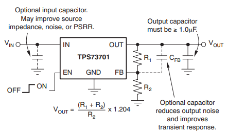
TO IMPROVE PSRR AND NOISE PERFORMANCE ,which layout is good?
Will the quality of Option 2 be very  poor?

thanks a lot

1、Input and output filter capacitors and feedback circuit are placed on the same layer with the IC 373,as shown in the figure below

Put more GND Via under the IC pad。

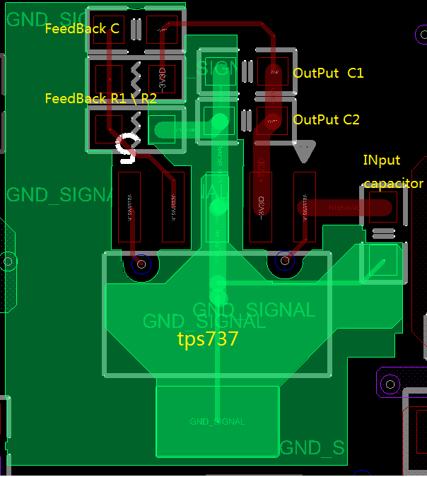
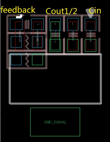
2、In order to save space, the IC TPS737 is placed on the top layer, and the input and output capacitors and feedback circuits are placed on the bottom layer . they are connected through vias.

in the picture bellow ,the red pads are TPS737 which on the top layer , the blue PADS are capacitors which on the bottom layer.

  • Hello,

    Option 1 is preferred when trying to minimize the effects of noise.

    The shortest loop area should be used to optimize the frequency response of bulk and decoupling capacitors.
    The shortest loop area is almost always obtained by placing capacitors on the same layer as the IC they are decoupling.
    Exceptions to this (examples include processors where dozens of decoupling caps are placed) do not apply for linear regulators because of the limited decoupling capacitors that are placed. 
    Optimizing the placement of decoupling capacitors gives the best possible performance when the circuitry is subjected to Conducted EMI.

    Protecting against another noise mechanism (electric field coupling, also known as capacitive coupling) is done through placing a shield within the plane layers.
    An effective shield would be making layer 2 a ground or return copper plane.  If the linear regulator is floating, then the RTN of the LDO should be placed on layer two, directly underneath all LDO circuitry which share that return.  It is easier to place a shield when all of the components are on the same layer.  Pay particular attention to sensitive pins such as the feedback node - that pin should be well protected against noise and large transients.

    Thanks,

    - Stephen

  • Stephen, Thanks very much!

    I will try to layout as option 1.

    By this sentence   "Exceptions to this (examples include processors where dozens of decoupling caps are placed) do not apply for linear regulators because of the limited decoupling capacitors that are placed. "

    do  you  mean , If there are many filter capacitors in the circuit, it is not necessary to limit all capacitors to the same layer? why you emphasize do not apply for  "linear regulators"?  The TPS737 is a linear regulators.

    thanks a lot.

  • I included that statement because linear regulators power devices, and sometimes the guidance for those devices might be a little different.  For a large ball grid array based FPGA the guidance might be to place the decoupling on the other side of the board, due to the large quantity of capacitors involved among other reasons.  A linear regulator usually does not have many capacitors to support it, so that is why the layout option 1 is the optimum for a linear regulator.

    Thanks,

    - Stephen

  • Dear,Stephen.

    Ok, I get it. Thanks very much.

    (*^▽^*)