This thread has been locked.

If you have a related question, please click the "Ask a related question" button in the top right corner. The newly created question will be automatically linked to this question.

WEBENCH® Tools/LM3478: Glitches and noise - PCB layout

Part Number: LM3478
Other Parts Discussed in Thread: LM3488

Tool/software: WEBENCH® Design Tools

Dear Youhao,

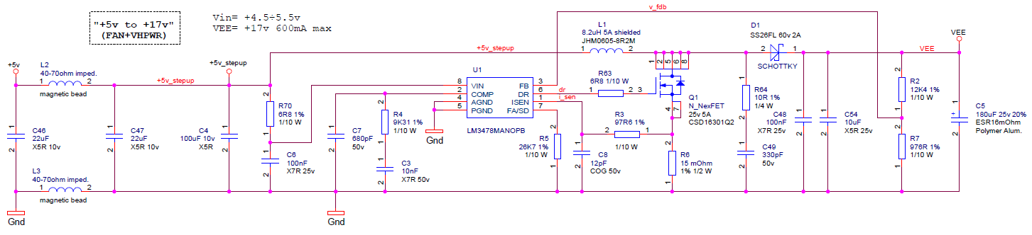
I contacted you 1 month ago to solve glitches/noise/EMC problems related to the LM3478 step-up.

Following the schematic diagram based on your suggestions and based on radiate EMC tests (passed).

NOTE:  the R64/C49 snubber filter values have not been tested yet.

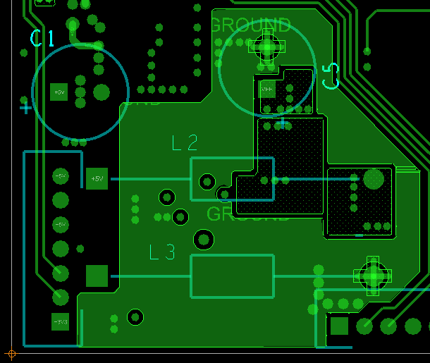
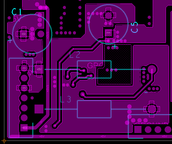
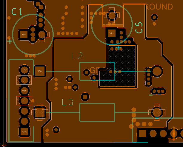
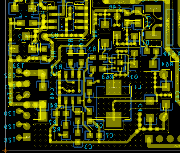
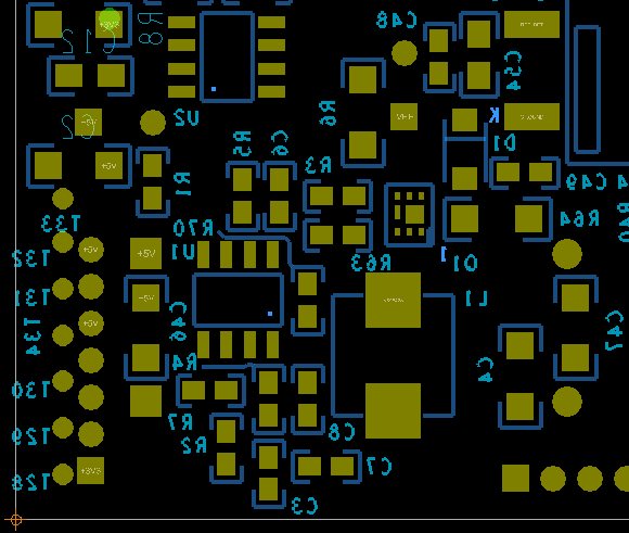
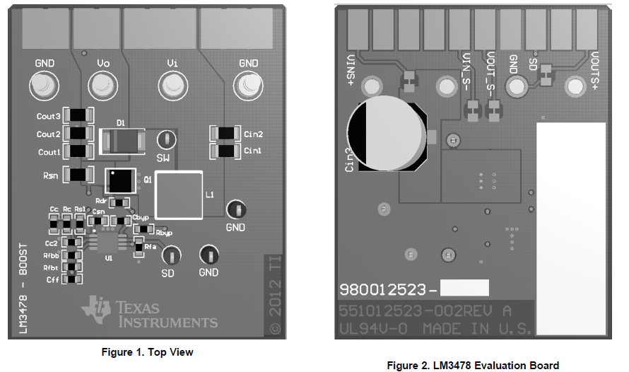
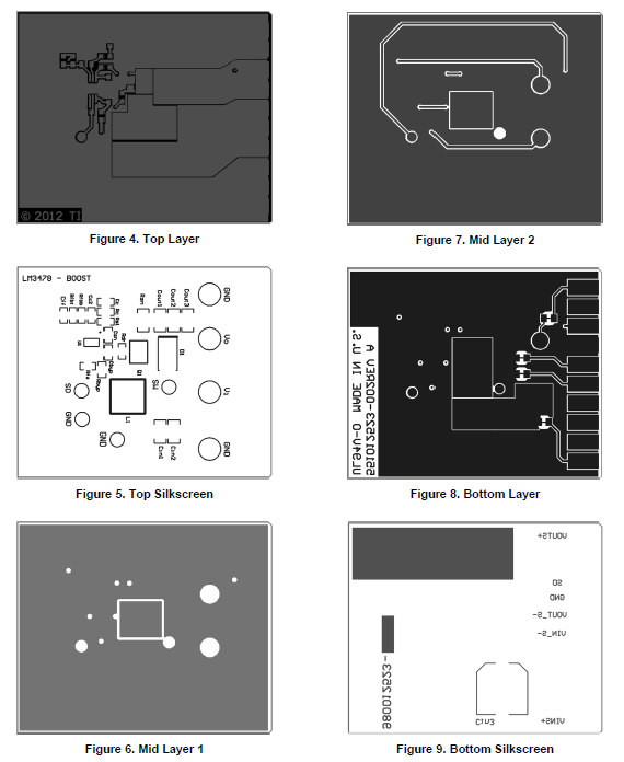
I'm actually drawing the PCB layout (4 layer) based on the attached TI user guide (AN-1204 LM3478/LM3488 Evaluation Board,  SNVA656A–June 2012–Revised October 2013)

. As suggested inside, I've drawn the PCB tracks wide & short, following same approach showed at pag. 5-6 and 10-11 (GND plane on all the 4 layers).

Below, you could find the PCB layer pictures and component silkscreen.

May you help me about the below question, please?

-  in your opinion, the PCB layout approach showed in to the TI user guide is a good method?

-  I've drawn a dedicated copper area on all the 4 PCB layers, for the L1 inductor/Q1 nexfet/D1 shottcky net, connecting them together with vias but keeping them separetd from the rest of the planes; do you agree about this approach?

-  I've drawn 4 GND dedicated planes (4 layer) connected together through vias in the following points: close to the L3-pin2, close to E-cap C5, close to U1; that planes reach the main GND track of the board circuit, only trough the vias close to E-cap C5;  is correct this approach ?

Please let me know if the explanation above is not clear.

Thanks in advance

Alessio


  • Hi Allesio,

    First, congratulations to you for passing the EMI test. 

    Regarding your new layout review, please allow us sometime.  Will try to get back to you by Friday this week.

    Thanks,

    Youhao Xi, Applications Engineering

  • Dear Youhao,

    Thank you very much

    Waiting for your kindly replay

    Regards

    Alessio.

  • Hi Alessio,

    Here are my comments.

    First, the PCB layout approach showed in to the TI user guide is not bad, in my opinion. Especially the placement and routing of the MOSFET, Rcs, Diode, and Cout.  The switching current (ac components) flows through these components, it is critical to keep these part tight and close, and guide the ac current to flow straightforward without much zigzagging and also without enclosing much spatial area.  Please also note that our EVM is basically a board to demonstrate the IC features and functions.  To be convenient for customer to probe, the EVM is usually places loosely. For your final product, you can follow the EVM layout pattern but fine tuning to make it tight and better is encouraged.

    Okay, back to your layout.  Regarding the said ac current route, your MOSFET and Rcs do not align, causing the current path to be zigzagging.  

    C5's pad is between C1 and D1, separating the two parts which actually should be closed to each other for the sake of above mentioned ac current loop. C5 should be moved outside that area. 

    The gate drive trace is zigzagging.  Note that the gate drive current path goes through Rcs (your R6).  If you trace the current from DR pin through the circuit back to the PGND pin, you can see a large spatial area is enclosed. The gate drive signal has high pulsing current and such a current loop can cause radiated EMI.  Please re-route it such that the area enclosed by the trace is minimal.

    R3 should be closer to the IC pin other than to the Rcs.  C8 ground trace should be directly tied to the IC GND pin, other taking a long trace to there. 

    I would R5 counterclockwise by 90 degree (top view), then its GND pad has shorter distance to the ground pins.

    Thanks,

    Youhao

  • Dear Youhao,

    Thank you very much for your detailed replay.Really appreciated.

    I'm going to implement your suggestions on the PCB layout.

    Kind Regards

    Alessio

  • Dear Youhao,

    Sorry, I miss one of your suggestions (probably a typing error).

    no C1 in the schematic; close to C5 E-cap pins, to the right, there are C48 and C54 and to the left R6

    (?)

    " .... C5's pad is between C1 and D1, separating the two parts which actually should be closed to each other for the sake of above mentioned ac current loop. C5 should be moved outside that area. "

    Thanks

    Alessio

  • Sorry it was a typo. I meant R6.  C5 hols forces R6 to be further left.  R6 could be next to C48//C54 and D1 ac current can flow through a tight route without enclose much area.

    Sorry for the confusion.  

  • Dear Youhao,

    Clear. Noted.

    Thank you again for the help

    Regards

    Alessio.

  • Thanks, Alessio.  Let me close the thread here, and you are welcome to create a new post if you have new questions.

    Good luck with your project.

    Thanks,

    Youhao