This thread has been locked.

If you have a related question, please click the "Ask a related question" button in the top right corner. The newly created question will be automatically linked to this question.

RE: TPS63070EVM-693: Adding Snubber to Reduce Output Ripple Voltage

Other Parts Discussed in Thread: TPS63070, TPS63070EVM-693

Hi Minqiu-san,

I have an additional question.
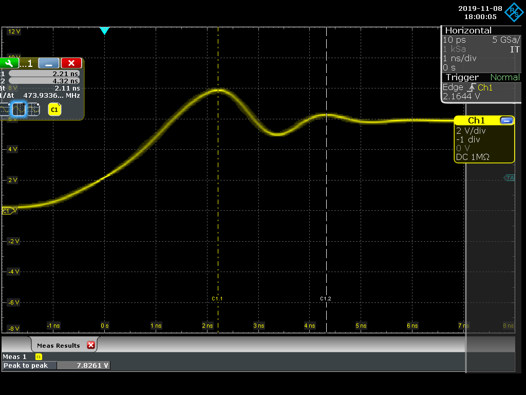
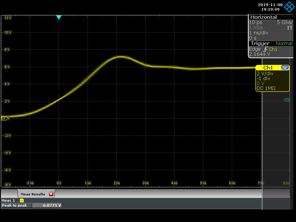
Could you please let me know if there is a fundamental solution without adding the ferrite beads to reduce the switching noise ?
For example, it would be very helpful for me if there is a workaround such as adding RC snubber circuit to the switching node since the switching noise couldn't be reduced even if the small size capacitors is added to the output node.

Best regards,
Kato

  • Hi Kato-San:

    May I know what's the load for customer? And what's the purpose care about the noise?

    Different need has different solution. In some cases, they don't consider too much about the noise, as it deliver little energy. 

  • Hi Minqiu-san,

    Thank you for your continuous support.

    I would like to apply the RC snubber circuit for TPS63070 to reduce the switching noise which is generated by TPS63070 itself.
    So, have you ever improved switching noise with RC snubber circuits for TPS63070 ?

    Best regards,
    Kato

  • Hi Kato-san:

    Honestly speaking, I'm not sure how much noise is caused by the measurement and setup, how much noise caused by real circuit. So for general application, observe the waveform under 20Mhz bandwidth is recommended.


    For snubber, you could check the application note:http://www.ti.com/litv/pdf/slva255

    The parameter depends on the surrounding components and layout. And the target should depends on your needs.

  • Hi Minqiu-san,

    Unfortunately, I cannot access above link for the application note. So, could you please tell me the link again.
    Additionally, please let me know if you have any ideas to reduce the switching noise without the ferrite beads on TPS63070EVM-693.

    Best regards,
    Kato

  • Hi Kato-san:

    Please check the link again.http://www.ti.com/lit/an/slva255/slva255.pdf

    The major principle to reduce the switch noise is :

    1. Reduce the parasitic parameters. (With good layout, high frequency Cin/Cout, minimum route, and so on)

    2. Add snubber

    3.Add ferrite beads

  • Hi Minqiu-san,

    Thank you for the information.

    I just got the application note, so I have an additional question.
    There is mentioned regarding the boost converter in the application note , but TPS63070 is buck-boost converter. So, should the snubber circuit added both "between L1 and GND" and "between L2 and GND" if adding the RC snubber circuit on EVM ?

    Best regards,
    Kato

  • Hi Sadanori-san:

    As your application will major operate in Boost mode, you could add it "L2 to GND"

  • Hi Minqiu-san,

    Thank you for your advice.

    Should the RC snubber circuit be added to "L1 to GND" to reduce the switching noise on Vin side if using TPS63070 as the buck converter ?

    Best regards,
    Kato

  • Hello Kato-san,

    In general I would recommend to first test with high-frequency capacitors connected extremely close to the IC on the input and output. These capacitors need to still have a capacitive behavior at the ringing frequency. For this it is necessary to measure the ringing on the customer application as it is very dependent on the layout and the used inductor. We have seen good results if the right capacitor is selected.

    If the customer wants to add a snubber, the one from L1 to GND will reduce the ringing on the input side and the one on L2 to GND will reduce the ringing on the output side.

    Would you please ask the customer how the ringing influences his design? What exactly is the problem he wants to solve?

  • Hi Brigitte-san,

    Thank you for the information.

    We just suggested to add the RC snubber circuit to our customer since the switching noise couldn't be reduced even if the small size capacitors is added to the output node.
    He feels that the output ripple voltage(620.89mVpp) is too higher as a issue with EVM.

    Best regards,
    Kato

  • Hi Brigitte-san and Minqiu-san,

    Our customer added RC snubber to "L2 to GND" on TPS63070EVM-693, but the switching noise on the switching node(L2 pin) has improved, but the switching noise on the output node(VOUT pin) hasn't improved yet.
    So, could you please confirm just in case whether this symptom can replicate as I don't have TPS63070EVM-693 ?
    Additionally, please tell me the RC snubber values to improve the switching noise on the output node.

    Best regards,
    Kato

  • Hi Kato-san,

    It's a public holiday here, so on Monday I will get back to you when I try using a snubber or a smaller output capacitor on the EVM. Sorry for the delay.

    Thanks and regards,
    Milos

  • Hi Milos-san,

    Thank you for following me.

    I am looking forward to getting the detailed information next Monday.

    Best regards,
    Kato

  • Hi Milos-san,

    Sorry for rushing you but please let me know if you have any updates.

    Best regards,
    Kato

  • Hi Kato-san,

    I am sorry for the delay, I will get to you in a few hours with the recommended snubber values for the TPS63070 EVM.

    I had to split the thread since the original one was resolved, and this is a new request.

    Best regards,
    Milos 

  • Hi Kato-san,

    I recommend 180 pF + 3.6 Ω on L2. This damped the oscillations and reduced the overshoot by half. Note, this was for conditions you mentioned in your previous thread: Vin = 4 V, Vout = 5 V, Iout = 1 A, and valid for the EVM. 

    Before:


    After:


    Best regards,
    Milos

  • Hi Milos-san,

    Sorry for overlooking your post.

    I would like to confirm just in case, but are these monitored waveforms for the L2 node ?
    If yes, the purpose is to reduce the ripple voltage of the output voltage VOUT, so please provide a screenshot of the output voltage VOUT.

    Best regards,
    Kato

  • Hi Kato-san,

    Here is the output ripple:

    Measured on C4, with a 1-GHz active differential probe, without bandwidth limiting:


    Measured on C7:


    These spikes are very short (ns or so) and are difficult to get rid off when measuring with full bandwidth, since some part is due to pickup by the measurement loop of the probe tip. It can be reduced by placing small (few nF) high frequency capacitor as close as possible to VOUT. Normally these spikes can be neglected, and the output voltage observed using the 20-MHz filter is:


    Best regards,
    Milos

  • Hi Milos-san,

    Thank you for your strong support.

    I understand and will inform this information to our customer. So, I will contact you again if I get additional qestions.

    Best regards,
    Kato

  • Hi Milos-san,

    I would like to confirm just in case, so could you please tell me the output load condition ?
    Is the load 50Ω of the probe ?
    Additionally, is the same result obtained when the load current is 1A ?

    Best regards,
    Kato

  • Hi Kato-san,

    The load is always 1 A. The input impedance of the probe is 1 MΩ || 0.6 pF (R&S RT-ZD10).

    Let us know if you need any other measurements.

    Best regards,
    Milos

  • Hi Milos-san,

    Thank you for the information.

    It seems that ch1 probe setting is DC 50Ω for the output voltage VOUT.

    Best regards,
    Kato

  • Hi Kato-san,

    Yes, the scope input is 50 Ω, but I used an active probe. The active probes have a built in amplifier. The probe amplifier has a high input impedance, and the output of the probe amplifier is for 50 Ω input, so the scope automatically adjusts Ch1 input for the probe output (both the scope and the probe are R&S).

    As far as the device-under-test is concerned, it sees only the high input impedance of the probe (i.e. the built in probe amplifier).

    I hope this is more clear now. 

    Best regards,
    Milos

  • Hi Milos-san,

    I understand and greatly appreciate your cooperation.

    Best regards,
    Kato