


We've been in production with this part for 8 years.
Our new PCB ASSY manufacturer is having issues with air bubbles under the part between the DAP and the PCB. We are having overheat issues on some channels on our PCB during burn in.
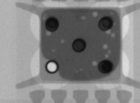
Here's an example an xray from one of the failed boards, I do not know at this time if this is an actual failed channel, but it does show how the solder has wicked away from the DAP and how air bubbles form between the DAP and the PCB.
The manufacturer has asked if 80% coverage is adequate.
Can TI provide me with a guideline on how much coverage is required for a part that is operating to worst case specification?
Thanks.
