This thread has been locked.

If you have a related question, please click the "Ask a related question" button in the top right corner. The newly created question will be automatically linked to this question.

TLV61046A: TLV61046A Output Lower than expected

Part Number: TLV61046A

Hi

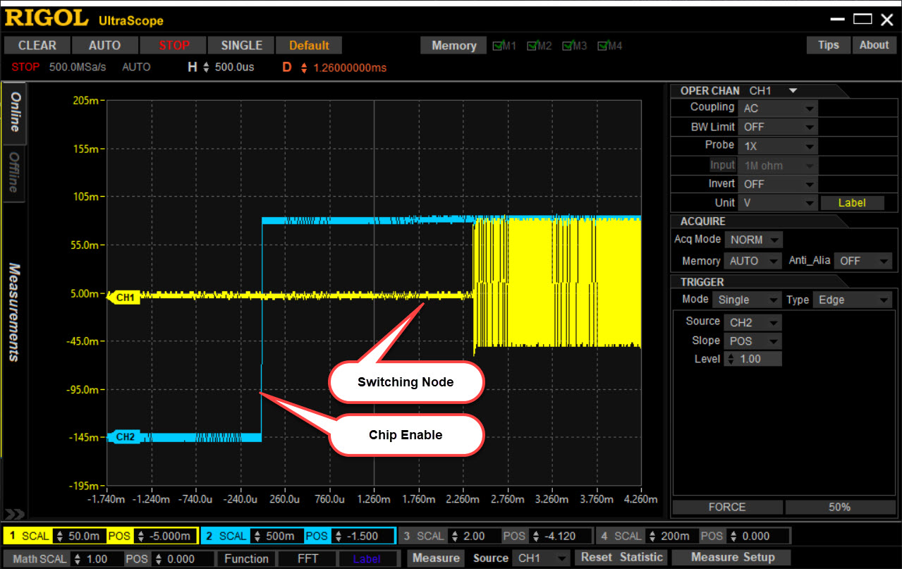
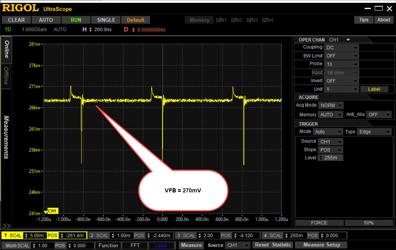
We have a new design using the TLV61046A which is not generating the expected output voltage, the output level is coming up to roughly 4.3V however no higher, with no output load attached.

The enable signal is set at around 2.2V which is above the threshold listed for the enable pin, it does also appear to turn the output on/off.

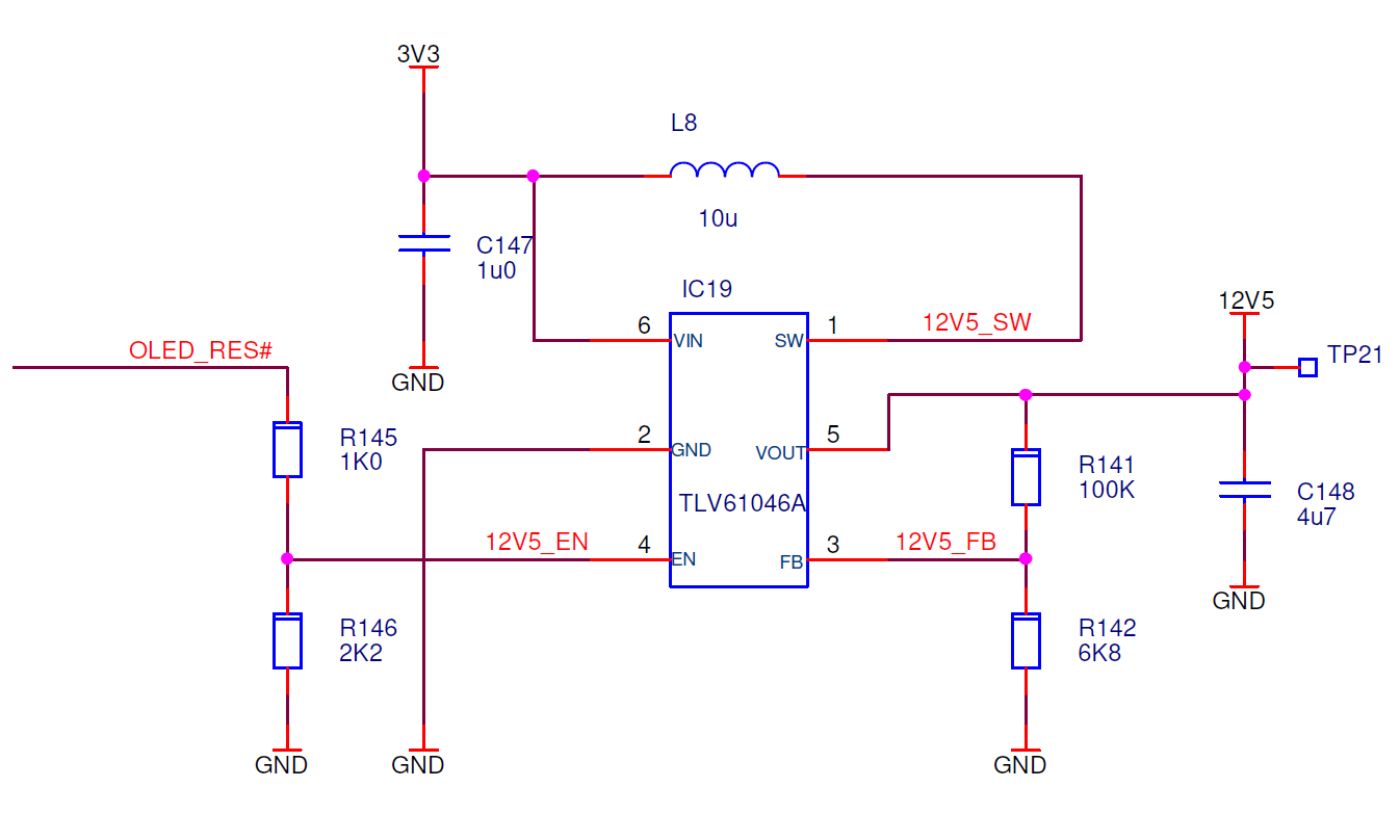
I've seen that most of the TI reference designs use 1M ohm for R141, is there a specific reason for this?

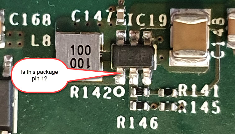
We also have a concern over the orientation of the part, would you please confirm the pin 1 location, there are many marks on the part none of which match the TI document DBV0006A pin 1 location "index area".

Any advice you can provide would be appreciated.


Regards

Malcolm

  • Hi Mal

    the pin position is correct. The pin 1 is in the left bottom of the IC from top view.

    is the bebahior found in every system board? what is output current when VOUT=4.2V.

    could you help to measure the waveform the VIN, VOUT and FB pin.

  • Hi Jasper

    The output condition with Vout approx 4.2V is with no load connected.

    I've taken some scope traces showing the various waveforms, also with respect to the enable signal.

    I have only one board right now however will have more in a few days.

    Chip Enable to Switching Node

    Chip Enable to Input Voltage, no droop observed.

    Feedback Voltage, measurements taken with a passive probe so noise pickup is likely.

    Output Voltage

    Inductor Switching Node

    PCB Layout – vias connected to solid planes on lower layers, red traces are on the top layer, blue trace on inner signal layer, all signals are ground referenced.

    Please let me know if you require any further information or have any suggestions on changes to make to the design.  I added additional input capacitance however this made no difference, I also use 1M and 68.1k feedback resistors for R142 and R141 however this also made no difference.  I was going to try a different inductor, the current inductor is a Wurth 74438336100 (katalog.we-online.com/.../74438336100.pdf)

    Regards

    Malcolm

  • Hi Malcolm,

    at EN=L, the SW pin voltage should be equal to VIN voltage. i'm thinking if the inductor is broken.

    could you measure the resistance between VIN and SW pin using multi-meter to confirm this? and try to renew the inductor.

  • Hi Malcolm,

    what is the update for this case? 

  • Hi Jasper

    I received two additional boards from the factory and these had a correct 12.5V output, so it would seem that there was a component issue with the first board we tested.

    I am expecting seven additional boards back from production tomorrow so once I have been able to validate the 12.5V supply on these boards is operating correctly I can close the case.

    With regards to the feedback resistors ours are currently 100k and 6k8, other than a higher current draw from the supply voltage to the feedback path are there any issues with this?  I've seen most of the TI reference designs use 1M and 68k however I assume this is to limit current consumption for battery powered devices.

    Regards

    Malcolm

  • Hi Malcolm,

    your understanding is correct. the reason to use large feedback resistor is to reduce the power loss.

    I closed the post. if you still see problem in the other board, just reply below.