This thread has been locked.

If you have a related question, please click the "Ask a related question" button in the top right corner. The newly created question will be automatically linked to this question.

UCC27211: Wrong LO and HO waveforms

Part Number: UCC27211

I am adoperating 2 UCC27211 gate driver in a DCDC current controller, the LI and HI inputs are fed by the outputs of a LT3741 controller and LO HO outputs are driving 4 IRL60B216 as it can be seen in this attachment

the inputs of the gate drivers are correctly driven but their outputs are not, the same error can be seen in both drivers

LI and LO:

HI and HO:
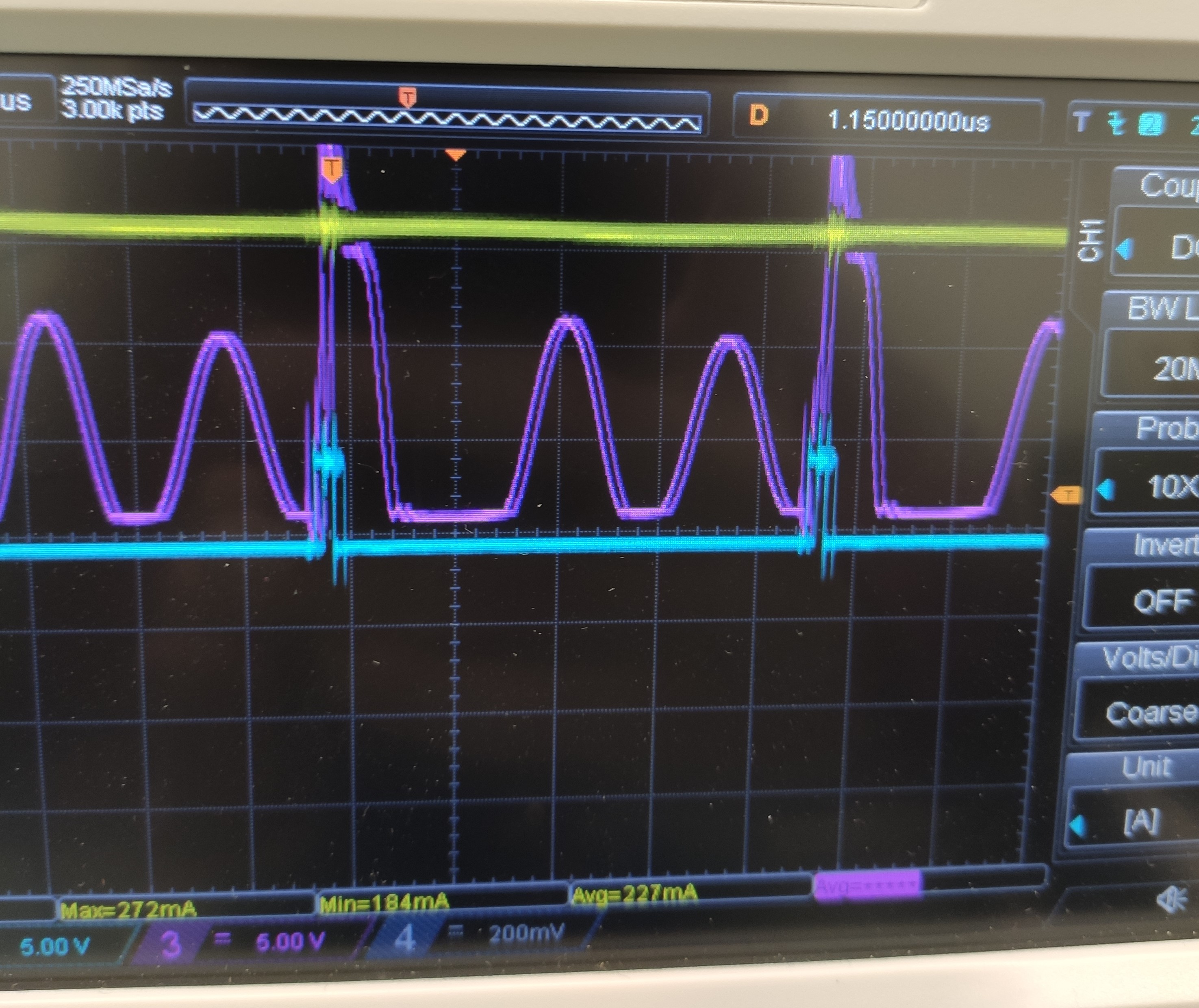
Light blue waveforms are the inputs of the UCC and violet waveforms are taken directly at the MOSFET's gates

Speaking about the Low side, i wondered about some voltage drop due to high driver current on the little resistances in series with the gate and i actually noticed that probing directly at the output of the driver

the square wave reaches like 10V (NOT 12V as it should be!!!); hence i tried to modify the value of the resistances but with poor results, i actually also tried to place a 0ohm instead so as to avoid the voltage drop but all I obtained was that 6V square wave clearly both at the gate and at the output of the drivers 

Speaking about the High side i wondered about a bad choice of the bootstrap C value, i increased it till 800nF but nothing changed

I also tried to increase the bypass capacitor value up to 4,7uF, to remove the SMDJ15CA and to place a resistor between MOSFET's gates and ground/HS, but still no result! So up to now i have no idea what to do

There is clearly some error in my design because i already used those drivers in a similar design with the same current controller but with different mosfets

  • Hello Matteo,

    Thank you for the interest in the UCC27211. I wanted to confirm a couple of things based on information provided. It appears the concern is with the HO output and the concern is the HO output amplitude being lower than expected. Please confirm.

    On thing to confirm is to see if the HB to HS bias is being charged to the voltage level that is expected. There will be a diode drop from VDD charging the HB-HS capacitance, and the expectation is that the switch node switches very close t ground to allow charging of the bootstrap capacitance.

    Can you confirm the voltage level on the HB pin and also probe the HO pin in the condition you show on the 1st plot, to confirm the voltage on the HB capacitance.

    Also can you confirm the switching of LO and HO in the condition you show in the 1st scope plot?

    The switching waveform looks to be soft switching and it may be that the switch node does not achieve close to ground. If the LO output is turned on, the low side MOSFET should saturate close to ground to allow bootstrap capacitor charging.

    Confirm if this addresses your concerns, or you can post additional questions on this thread.

    Regards,

  • Richard Herring said:

    Hello Matteo,

    Thank you for the interest in the UCC27211. I wanted to confirm a couple of things based on information provided. It appears the concern is with the HO output and the concern is the HO output amplitude being lower than expected. Please confirm.

    On thing to confirm is to see if the HB to HS bias is being charged to the voltage level that is expected. There will be a diode drop from VDD charging the HB-HS capacitance, and the expectation is that the switch node switches very close t ground to allow charging of the bootstrap capacitance.

    Can you confirm the voltage level on the HB pin and also probe the HO pin in the condition you show on the 1st plot, to confirm the voltage on the HB capacitance.

    Also can you confirm the switching of LO and HO in the condition you show in the 1st scope plot?

    The switching waveform looks to be soft switching and it may be that the switch node does not achieve close to ground. If the LO output is turned on, the low side MOSFET should saturate close to ground to allow bootstrap capacitor charging.

    Confirm if this addresses your concerns, or you can post additional questions on this thread.

    Regards,

    Hello, thanks for answering me promptly

    No, the concern is both for the LO and the HO output; the first plot represent LI (light blue) and LO (violet), LO is clearly lower than expected

    then the second plot represent HI(light blue) and HO (violet), here HO has a strange behaviour i totally can understand, it's like it tries to reach 12V and the falls down and then try again etc..

  • Hello Matteo,

    For the LO plot in the 1st waveform. Can you confirm how LO looks with wider pulse width? With the narrow pulse width, it is not clear if the LO level is just reaching the miller plateau before the pulse width is over. If the pulse width is wider does LO reach the expected amplitude.

    For HO it is possible the Ho drop is from the Mosfet switching and miller charge of the high side mosfet causing the HO to drop when the high side Vds is switching and causing the MOSFET miller charge to transfer to the MOSFET Vgs. Can you show some waveforms with somewhat wider pulse widths on LO and HO to see what LO and HO looks like with longer time for the MOSFET Vgs to transition?

    Confirm if this addresses your concerns or you can post additional questions on this thread.

    Regards,