This thread has been locked.

If you have a related question, please click the "Ask a related question" button in the top right corner. The newly created question will be automatically linked to this question.

WEBENCH® Tools/LM5022: LM5022 maximum output current

Part Number: LM5022

Tool/software: WEBENCH® Design Tools

Hello,

I need to use the LM5022 as a step-up to convert 9..16.6V to 34.8V@1.17A or to 34.8V@0.5A.

According to the 8.1's Application Information section, the LM5022 is available to delivery 40V@0.5A from 9..16V.
But the webench confuse myself because it's tittle bar let me think is it possible to have a output of 34.8V@1.17A.

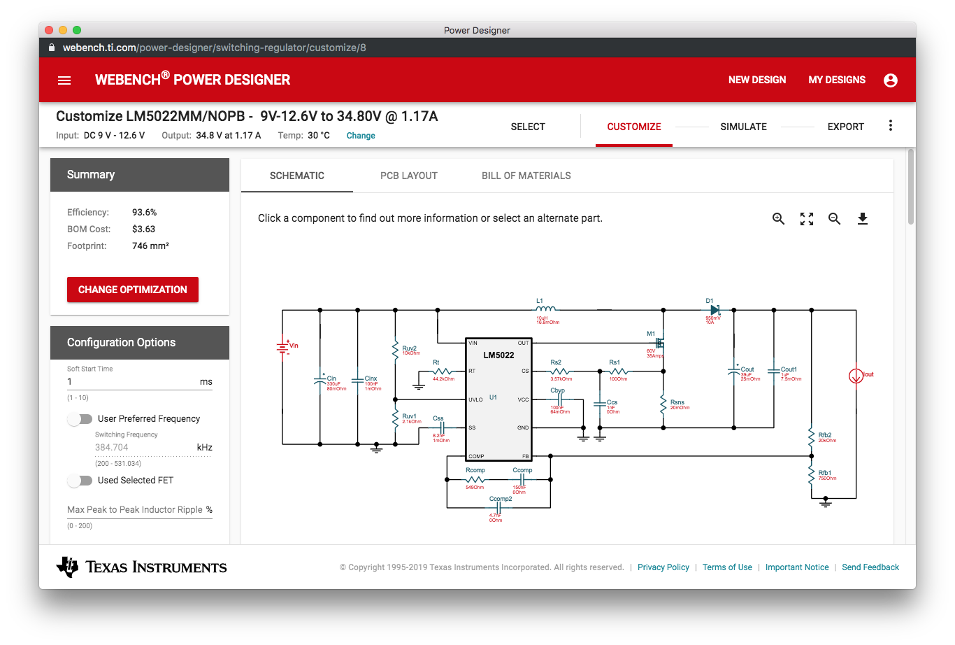
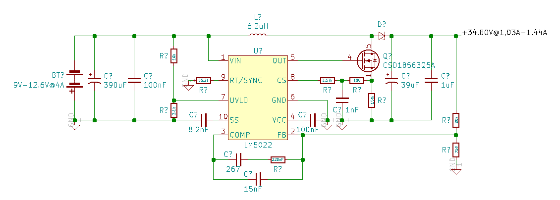
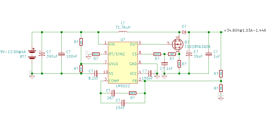
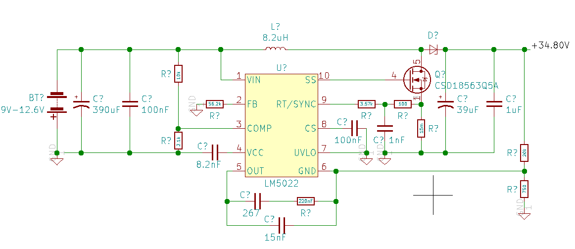
Soo, according to the datasheet and the webench I have drawed this shematic:

My questions are:

  • A output of 34.8V@1.17A or 34.8V@0.5A is possible? How can I calculate maximum current output available?

Thank's for your help.

adjivas

  • Hi Adjivas,

    Thanks for considering the LM5022 in your design. I've attached my responses below: 

    Q: Is a output of 34.8V @ 1.17A or 34.8V @ 0.5A possible?

    The application section discusses how to design a circuit to generate a 40V rail that can output 0.5A as an example. 

    I've attached some reference designs within your power requirements (20-40W) below that you can use to help you get started.

    http://www.ti.com/tool/PMP20497

    http://www.ti.com/tool/PMP20070

    Q: How can I calculate maximum current output available?

    To calculate the maximum output current, you will need to know the maximum input current and desired efficiency. Then, you can calculate the output current since n*P_in = P_out, where n = efficiency, P_in is input power, and P_out is output power. 

    The maximum output current available is not dependent on the controller, instead- it is determined by the ratings of your components like your inductor, FET and diode.  

    Additional notes:

    In your schematic, your input supply is connected backwards. 

    Please let me know if I answered your questions.

    Thanks,

    Richard

  • Hello Richard,

    Thank you for your reply, that has advanced myself.

    My maximum discharger is: 4A.
    Without consider the efficiency my results are:

    • n * 12,6V * 4A = n * 34,8V * 1,44A
    • n * 9V * 4A =  n * 34,8V * 1,03A

    I have also fixed my schematic:

    The values was sourced and calculated by the webench's tool.

    My last questions are:

    • How can I calculate the adapted inductor value?
    • Should I adapt other components value?

    adjivas

  • Hi adjivas,

    I still think your input source (BT) is connected backwards. Please flip the source so that the positive sign is connected to the positive terminal of the 390uF capacitor. 

    As for selection of power components, I think you should refer to the guide I listed below, which will help you modify the components value as needed.

    http://www.ti.com/lit/an/slva372c/slva372c.pdf

    The LM5022 datasheet has section 8.2.2.10, which can be used to help you calculate the control loop compensation values.

    I hope this helps!

    Thanks,

    Richard

  • Oups! That fixed, I have flipped the BT and adjusted the inductance.

    Your link http://www.ti.com/lit/an/slva372c/slva372c.pdf was many helped me.
    I have adapted the inductance L1 at 71,76uH according to this calculation:

    • Equation 14: D=1-((9Vin(min)*0.85n)/34.80V=0,78D
    • Equation 19: ΔIL=0.2fs*1.03A*34.80V/12,6V=0,56ΔIL
    • Equation 18: L=(12,6Vin*(34,80Vout-12,6Vin))/(0,56ΔIL*0.2fs*34,80Vout)=71,76uH

    Your 8.2.2.10 section link https://www.ti.com/lit/ds/symlink/lm5022.pdf#%5B%7B%22num%22%3A238%2C%22gen%22%3A0%7D%2C%7B%22name%22%3A%22XYZ%22%7D%2C0%2C199.8%2C0%5D let me understand I will should adjust the values of C1, C2, R1 with equation 55, equation 54 and equation 53.

    Did I understand everything correctly?
    I will recheck my read of your documents tomorrow, thank's for your help.

  • Hi adjivas,

    Yes, you have understood how to select the inductor correctly and you can use equation 53,54,55 to select compensation components. However, you will need to iterate through designs until you have reached your desired result. 

    According to the calculations, your inductor value is very large, so I would recommend increasing the switching frequency (modifying the RT resistor) to reduce that value to minimize cost and size constraints. In the first link (SLVA372C), I would advise looking at the references section so you have more resources to help you design your boost converter.

    Let me know if you have any questions. 

    Thanks,

    Richard

  • Hello Richard,

    According to the equation 53: R1=A*Rfb2.
    I suppose A=0.15 because it was mentioned by the example of the equation.
    According to the webench, Rfb2=750.
    So my R1's result is 112,5k. This differs from R1 webench tool's result which is 0ohm.

    Should I not change the value of A?
    Should I also adapt the Rfb1/Rfb2's resistance values?

    According to the equation 54: C2=1/(2π*R1*Fz1) where R1 is exprimed in ohm.
    According to 6. Fz1=Flfp=ωLFP/2π. The example proposes Flfp=423Hz.

    What Flfp's frequency should I choice?

    According to the equation 55: C1=C2/(2π*C2*R1*Fp1-1). The example proposes Fp1=100kHz.

    What Fp1's frequency should I choice?

    According to your recommendation I have reduced the inductance at 27uH.

    • Equation 19: ΔIL=0.4fs*1.03A*34.80V/12,6V=0,56ΔIL=1,13
    • Equation 18: L=(12,6Vin*(34,80Vout-12,6Vin))/(1,13ΔIL*0.2fs*34,80Vout)=27uH

    I have used the 0.4fs value because is it inside the minimum switching frequency range of the converter mentionned at Equations to Calculate the Power Stage of a Boost Converter' section 8. Note that the fs unity isn't specified.

    According too Oscillator, Shutdown, and SYNC' section 7.4.1 I configure the RT/SYNC resistance with this equation: Rt=(1-8*10^-8*fsw)/(fsw*5.77*10^-11) where fsw is exprimed in Hz. Soo I has supposed fsw=fs=400000Hz where 0.4fs is exprimed in MHz. My result is 41,94k.

    Right I'm to suppose the fsw variable is exprimed in Hz?

    adjivas

  • Hi adjivas,

    Here are my responses to your questions:

    1) Should I not change the value of A?

    Your value of 'A' will depend on the gain of the power stage at the cross-over frequency. So the first step is to determine the cross-over frequency. Since you have a wide input range, I would recommend first determining the Right-half plane zero (RHPZ) frequency, and then making your cross-over 1/5 of it or smaller. 

    Once you do this, you should take the negative of that gain and convert that value in dB to a linear gain. Please see steps 1->3 on page 24 of the datasheet for further insight. 

    2) Should I also adapt the Rfb1/Rfb2's resistance values?

    Your value of Rfb2 should be in between 10k Ohm and 100k Ohm for practicality. Once you selected a Rfb2 value, your value of Rfb1 should be selected such that the voltage seen at the FB pin is equal to the voltage reference (1.25V). Your values from Webench are fine.

    3) What Flfp's frequency should I choice?

    F_lpf is dependent on your power stage and selection of power components. Please refer to equation 46. 

    4) What Fp1's frequency should I choice?

    I recommend following the datasheet's recommendation, which is to be 1/5 of the switching frequency. 

    5) Inductor Selection (Reduced to 27uH)

    Inductance still seems a bit high, but probably ok for your switching frequency. You can reduce it to minimize cost, size, power dissipation if you increased your switching frequency- but your switching losses will increase.

    6) I'm to suppose the fsw variable is exprimed in Hz?

    Fsw variable is supposed to be chosen as part of the input variables, and is in Hz. 

    Thanks,

    Richard