This thread has been locked.

If you have a related question, please click the "Ask a related question" button in the top right corner. The newly created question will be automatically linked to this question.

LMG1210: LMG1210 with -200V high side

Part Number: LMG1210

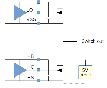
Hi-  We're designing a driver for a 0 to -200V application.  Having a bit of trouble envisioning exactly what topology and power supplies are needed.  See sketch attached.  For the "high side" switch, it seems clear.  HS is the negative HV supply, we can use a small floating DC/DC to provide 5V for HB and all is well using an N-MOSFET.

For the "low side" switch the topology is not obvious.  As drawing with an N-MOSFET there is no local ground to connect the driver to.  One could use a P-MOSFET but then LO would need to drive to -5V.

Any suggestions, or a pointer to an example application circuit for 0 to -200V drive?

Thanks,

Eric Hazen

  • Hi Eric,

    thanks for reaching out on LMG1210,

    Typically both FETs are NMOS for easy driving and rail to rail capability. Why choose PMOS? what application is this for motor drive?

    What voltage will be on VSS (source of low-side NFET or driver ground)? what voltage will be on the VBUS (drain of high-side NFET)?

    How come the high-side FET in your SBD is shown as the low-side? Typically HB-HS is shown on the upper portion of the half-bridge and LO-VSS is shown on the lower portion of the half-bridge as seen in page 1 of the LMG1210 datasheet ()

    The negative voltage capability of 1210 is limited by the HB-HS voltage as well as the bootstrap diode forward voltage. For example, using a -200V bus voltage (while VSS=0V) then a bootstrap diode cannot be used (due to BST voltage rating out of spec). If HS is at -200V, then HB should be at -195V. A bootstrap diode from BST to HB would have 195V of forward bias on it (since VDD is already charged to -195V and when 0V is applied to the switch node with the low-side FETs the diode forward bias becomes out of spec). This will cause the diode to blow up and the HB-HS voltage to go up and exceed the limit. If needing to power the high-side FET at -200V, you need an isolated supply for HB-HS while floating the BST pin. Let me know if you have any questions on this.

    Thanks,

  • Hi Jeff-

    Thanks for getting back to me.  The application is for a particle physics experiment; we're driving an electron gun which (along with it's floating power supply) must be pulsed from 0 to -200V, with a risetime of 50ns or so.  The load capacitance is around 100pF.  We did a design a number of years ago using a transformer-isolated driver and hoped to update it using the LMG1210.

    So, we need two switches; a switch to GND and a switch to -200V, driving a load which is largely capacitive load though there is some DC current flowing due to electron emission from the gun.   The "high side" switch I understand; we provide a floating 5V supply and do not use the bootstrap diode.

    My confusion is over the "low side" which which must switch to ground but tolerate 200V on the drain of the low-side MOSFET.  Obviously that would not work with an N-Channel MOSFET.

    To answer your specific questions:

    What voltage will be on VSS (source of low-side NFET or driver ground)? what voltage will be on the VBUS (drain of high-side NFET)?

    That is exactly my question.  If VSS (the source of the low-side MOSFET) is GND, then the drain of said MOSFET would swing to -200V when the high-side switch is on which would of course not work due to the drain-source diode.

    How come the high-side FET in your SBD is shown as the low-side? 

    Well, that's a matter of preference.  Typically I draw diagrams with positive voltages towards the top and negative voltages towards the bottom.

    Best,
    Eric

  • Hi Eric,

    Thanks for the update, do you have a schematic or simulation of this circuit for me to review?

    When you say drain-source diode do you mean MOSFETs intrinsic body diode? This seems to be the case for -200V on the drain of a MOSFET, it forward biases the body diode and cross conducts the FETs.

    A GaN FET by design does not exhibit the effects of a body diode however can still conduct in reverse.

    If not using a bootstrap diode then the limitation is not LMG1210 but it is to separately drive each FET with the switch node (drain of FET) going to -200V?

    Thanks,