This thread has been locked.

If you have a related question, please click the "Ask a related question" button in the top right corner. The newly created question will be automatically linked to this question.

LM22677: IC were damage after first power on or in burn-in test.

Part Number: LM22677

Hi ,

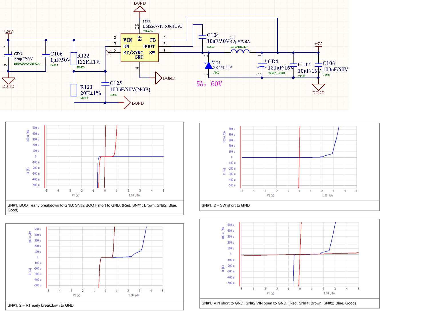
   Picture 1 is customer's last generation product and they had produced 10 kilo units without problem. Because they want to change brown-in voltage in new product,

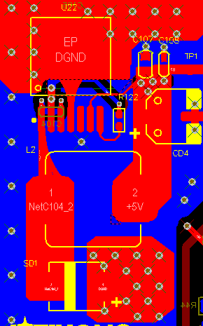
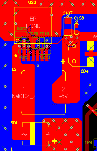
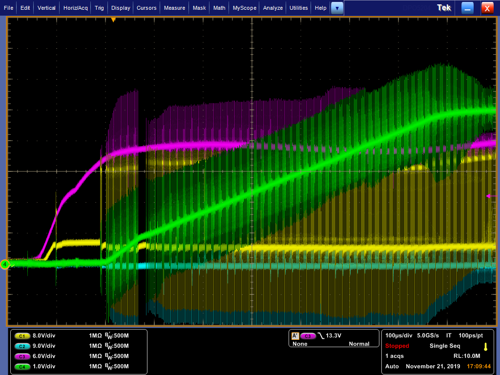
as picture 2 they modify the EN pin from a 470kohm pull-up to a voltage divider, and the other circuit is same as picture 1. Before they had faced voltage oscillation on

EN pin,it is solved by remove the cap connect on EN pin. Now voltage on EN pin is good ,but the chip still damage and the failure rate is 32pcs/192pcs.

Because customer using the same real of chips on mass product and new design so we don't think it is quality issue. Please help me to figure out what will cause this.

Thanks 

  • Attached picture 2 again

  • Hi Jeff,

    1. Do they use the same layout for the first and second design? I found the input loop which is composed by IC, diode, C106 is big in your layout.

    2. In pic 2, SN1 and SN2, both of them are broken? So VIN, SW, BOOT are all short to GND for the broken IC, right?

  • Hi Neal,

    1. Do they use the same layout for the first and second design? I found the input loop which is composed by IC, diode, C106 is big in your layout.

    As below picture1 and picture2, two layout and placement  are almost the same,they increase SW node copper area in new design. 

    2. In pic 2, SN1 and SN2, both of them are broken? So VIN, SW, BOOT are all short to GND for the broken IC, right?

    Yes, both SN1 and SN2 are broken.   In FA report the VIN of SN2 was open, but in customer factory most of broken chip are short to ground.

    Thanks

    Picture 1: First Design Layout without issue.

    Picture 2 : Second Design

  • Hi Jeff,

    For the original layout, I can't find C106. But I guess the input loop which is composed by IC, diode, C106 is also big.

    Does the device work in a condition, when the IC power off,  the input voltage drops very quickly? I'm thinking that during power off, if Vin is lower than Vo, current will flow the high side MOS's parasitic diode, and may damage the IC.

  • Hi Neal,

         As below picture, we don't see the voltage VIN less then vout condition on test fixture. And customer say they had many failure board happened

    during burn-in test. They do not have power on and power off  during burn-in test.  The ambiance temp is 55°C and they measure the top of the chip temp

    is about 77°C ~79°C. The total test time are 4 hours. 

        They want to reproduce the failure  phenomenon, so they rework the failure board. And do some testing like short vout、heating the chip (using heat gun)、

    full load power on、light load power on and ESD ,after all the testing the chip still work well. They could not reproduce failure  phenomenon. I had checked

    the smt manufacture is the same as first design. Do you have any idea to reproduce that? 

    Picture 1 and 2 were measurement from customer's board .

    Picture 3 and 4 were measurement from EVM board .

    They didn't using tip-and-barrel method to measurement so the waveform have glitch.

    CH1: BOOT

    CH2: SW

    CH3: VIN

    CH4: VOUT


    Customer's Board Power On


    Customer's Board Power Off

    EVM Power On

    EVM Power Off

  • Hi Jeff,

    This problem seems quite complex. Please send me email for further discussion. ( neal-zhang@ti.com )