This thread has been locked.

If you have a related question, please click the "Ask a related question" button in the top right corner. The newly created question will be automatically linked to this question.

UCC2897A: Facing issues in emi emc testing due to switching noise.

Part Number: UCC2897A

hi,

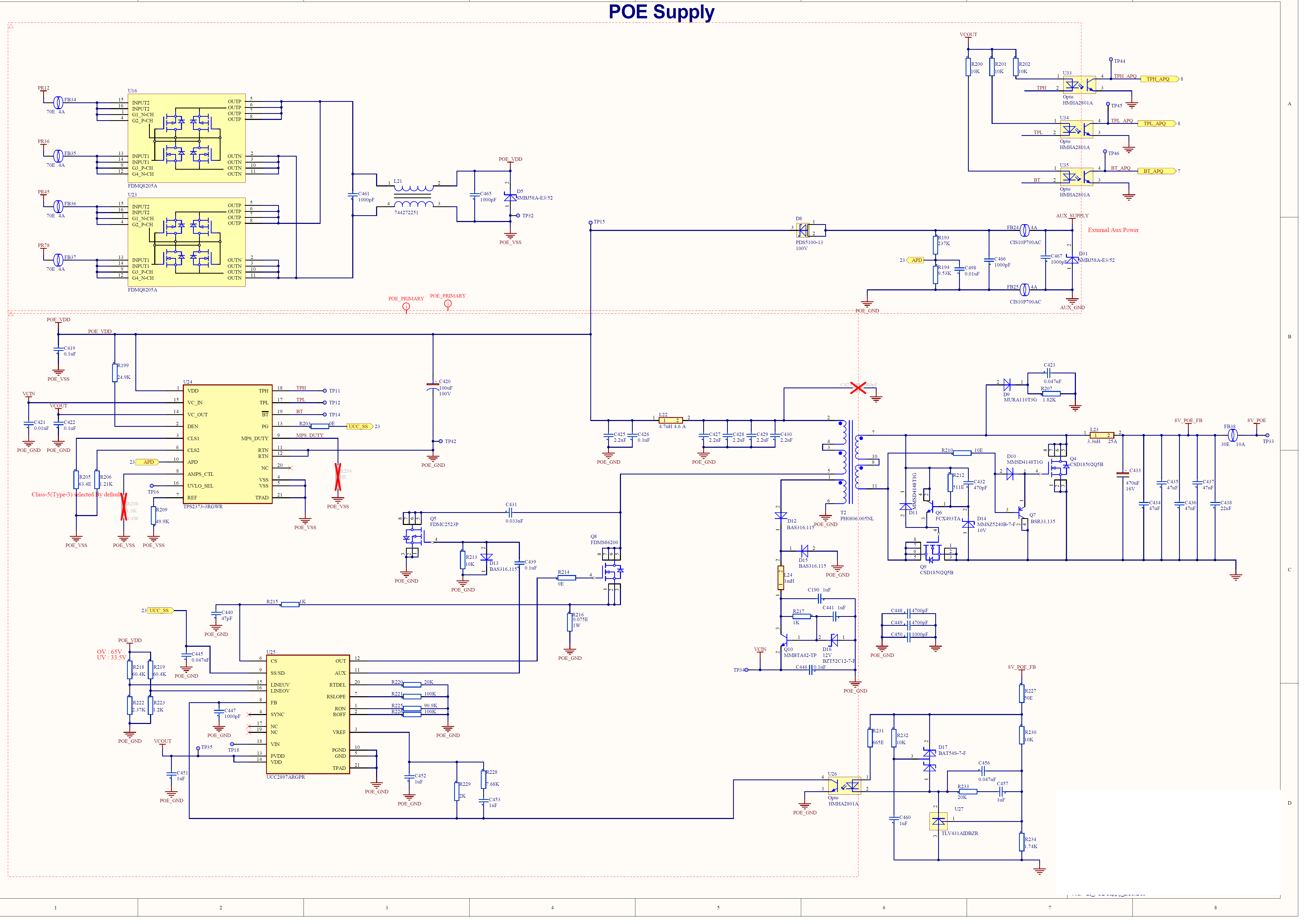
I am facing a issue in emi/emc testing as i have POE based Design using Ic TPS2373-3RGWR  with switching IC UCC2897ARGPR as the switching noise is coupling over the Ethernet cable and radiate due to this we are failing in emi/emc testing , due to the switching harmonics at 30Mhz - 1Ghz range the complete noise floor increased and fails, we have tried a couple of options but it never reduced but at last we tune the common mode choke then it shows some effect but not much.

I am attaching my schematic for the reference, please suggest the options so that we can pass the emi/emc prescan testing.

In this 1st one is with near feild probe and 3rd one is anechoic chamber result.

Regards,

Pankaj


  • Hi Pankaj Kanthaliya, an expert will reply you tomorrow.Thanks.—— Teng

  • Hi Pankaj,

    EMI is a system level issue. it related to filters design , PCB layout ,snubber circuit, components choose and so on.

    Here are some proposals for your case, you can try them:

    1. Don't know what kind of material of CM choke you are using . for high frequency noise suppress in your test waveforms 50~100M , I suggest you select NiZn CM choke rather than MnZi Choke ,

    2. The PCB layout : Shrink high Di/Dt current loop area . and high Dv/Dt nodes should be away from input filter circuits.

    3. Put the DC link ceramic capacitors as close as possible to Di/Dt loop .if possible try to use CBB capacitors in here.

    4. Shielding your transformer flux by copper foil and grounded it.

    5. You can use near field prober to find out the noise frequency and check if it's a hormonic of switching frequency or secondary side FETs reverse recovery noise and try to adjust your snubber .

    Hope can help you.

    Thanks.

  • Hi jaden,

    Thanks for the reply.

    Can you please elaborate the above points in our schematic, at which point you are taking about di/dt and filter caps and please suggest the snubber values with its reference designator in our schematic.

    your prompt replay would be highly appreciated.

    Regards,

    Pankaj

  • Hi Pankaj

    The high di/dt loop on primary side is Bulk filter caps -> Transformer primary winding ->main FET->GND, another di/dt loop is Bulk filter caps -> Transformer primary winding->Clamp cap->AUX FET ->GND. the main high di/dt on secondary side is  transformer winding ->rectifier FET ->output caps  and freewheel FET. The filter caps in your schematic are 2.2uF c427~c430. the schematic is indistinct I don't know if C427 is correct or not maybe it's C417, but anyway , the filter caps are close to your transformer. you have to make a trade off between EMI effect and efficiency to choose the snubber value ,  R=10ohm and C=470pF maybe a start point for your secondary side FETs.

    Thanks.

  • Hi Jaden,

    Thanks for the reply.

    Here i have attached the schematic for the better visibility in pdf format.

    please check once.

    4617.POE.pdf

  • Hi Pankaj,

    Thanks for sharing the schematic again , I don't have any more comments about it. if you have further questions, please create a new post.

    Thanks.