Hi all,
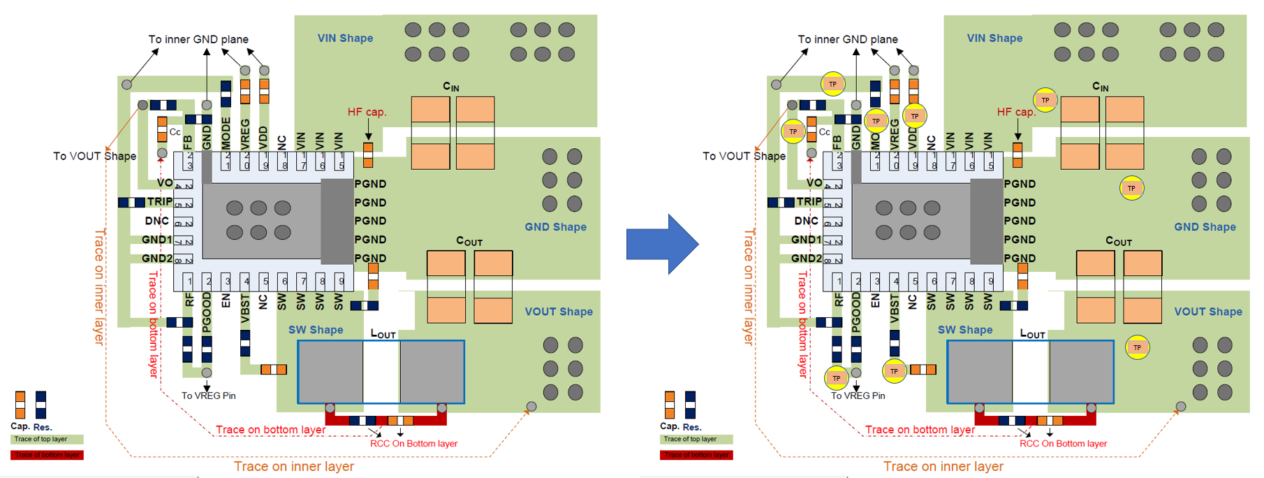
Regarding of test point, that we want to implement it for ICT function test in factory.
About TI’s each chip solution, do you have any concern which traces should not be added test point, example h/l gate trace, phase, sensing …
I think should added test point at source input voltage and end output voltage side for ICT only, right?
or don't care it!
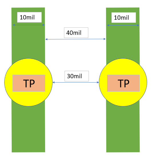
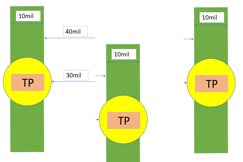
(1)The test point diameter is 20mil, if layout trace less than (ex : 10mil) whether can be add it?
(2)Will the ICT test cause ESD breakdown?