This thread has been locked.

If you have a related question, please click the "Ask a related question" button in the top right corner. The newly created question will be automatically linked to this question.

LM5088: Issues with output at high load

Part Number: LM5088

Hello,

For a project I am developing a DC/DC converter with the LM5088. Vin(min) = 9V, Vin(max)=60V, Vout=5V, Iout=8A. I made the design based upon the design that Webench provided me with.

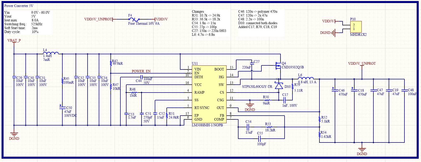
Below, a picture of the schematic can be seen.

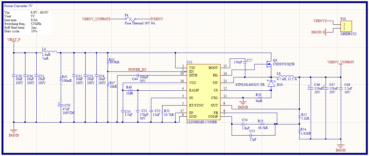
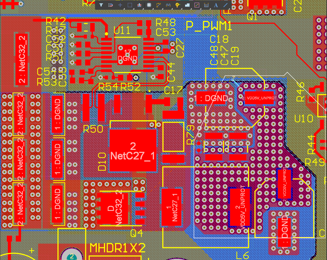
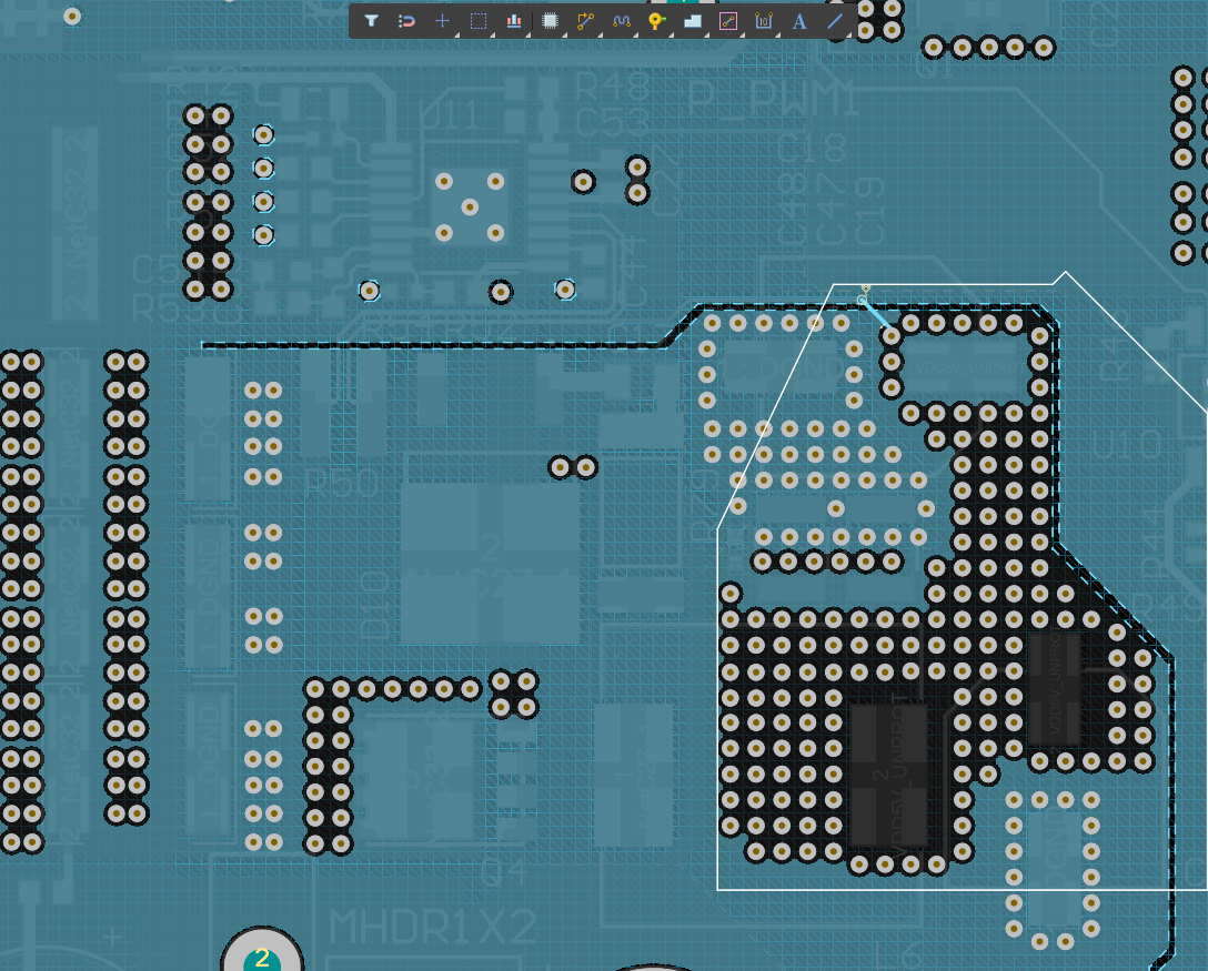
Also the PCB layout is provided below. I can provide you with entire PCB layout in mail if that helps.

I have the problem that the 5V output is not stable at high Vin(>20V) at high load (1R). When input voltage under or 16V, everything is fine and the output is stable 5V. However, when Vin increases from 16V to 20V the ripple gets worse, the converter starts making a high pitch noise and the dithering stops. The 5V output decreases and then drops to >3V.

At a load of >50R, all is fine. At every voltage from 9V to 60V the output is stable 5V.

The screenshot of the scope below shows the Source voltage during operation at 16V input voltage with 50R load.

As you can see, the switching is neat and constant. Also, dithering is present. This can be seen at the scope where the frequency changes but can obviously not be seen in the picture of the scope.

The screenshot below shows operation at 24V input at 1R load.

As you can see, the converter does not operate properly. Below, a zoomed in screenshot can be seen.

It can be seen that the switching pulses are not constant. Sometimes, a very short pulse is made. After multiple of these very short pulses, the converter shuts down for a certain period of time, as can be seen in the screenshot above.

I already tried to change compensation network to exactly what is placed on the LM5088 Evaluation Board but this did not help. Also I changed the output capacitors bigger/smaller and more/less electrolytic/MLCC to create less ESR but no success. Current sense resistor was made smaller (5mR) and bigger (10mR) to see if that made a difference. It did not make a difference and at high input voltages (>20V) the output is not stable 5V and drops to >3V (with heavy ripple)

I asked few different people with knowledge but none of them were able to find the problem. I hope very much that you are able to help me, as this is holding the project back a lot since I cannot conduct further tests with the PCBA. I would like to hear from you.

Thanks in advance!

  • Hi,

    We will have expert reply to you.

  • Hi,

    Do you know when an expert will reply?

    I am in kind of a hurry as I would like to test the rest of my project. I hope you can reply soon!

    Thanks in advance.

    Teun.

  • Hi Teun,

    Sorry the reply may be delayed since US holiday. 

    Please send email to me: neal-zhang@ti.com

  • Hi Teun,

    Please fill out and send the LM5088 quickstart calculator so we can check compensation: http://www.ti.com/product/LM5088/toolssoftware#devtools

    There may be some noise on the current sense as the traces are routed close to the SW trace coming from the boot cap. By the way, the boot cap shouldn't have this large a package. It should be 0603 and placed directly at the BOOT and SW pins.

    Also, the RAMP cap should be routed to AGND (pin 6), not through vias to the PGND connection at the large cap bank to the left of the controller. Similarly, the lower feedback resistor should be route to AGND, not the vias at the shunt resistor.

    Also important is to keep the ceramic input caps close to the FET/diode/shunt. Try connecting a 1uF cap from the drain of the FET to ground of the shunt to keep the high-frequency switched currents in a tight loop. See part 6 here for more detail on power stage PCB layout: http://www.how2power.com/other/EMI_Guide.php

    Regards,

    Tim

  • Dear Tim,

    Thank you for your reply.

    We did check the compensation network multiple times and also modified it to be exact the values of the AN-1913 LM5088 Evaluation Board. This did not help.

    You are right that the PCB layout is not ideal. Due to size and time constraints not enough attention has been paid to the design of this DC/DC converter. We did underestimate the design of a converter with these specifications.

    We will change and improve the PCB design so that we can get the power stage functioning correctly. Is it possible that you review the PCB layout from the converter? This would help us a lot to ensure we are not producing (another) not working PCB and thus reducing risk.

    I prefer to do this via email as it is easier to attach attachments etc., but here on the forum would also be fine.

    I hope to hear from you!

    Thanks in advance.

    Regards, Teun

  • Dear Timothy, 

    We have been improving the design. We would really like you to take a look and give us advice whether this design would function properly and if there could be other layout improvements. We tried to put the controller out of the high current loop and decrease big current loops overall. We also made some other improvements like snubber and output caps with lower ESR.

    I will post some screenshots of the design below. If you like, I can send the design files via mail to take a better look.

    Schematic:

    PCB:

    I hope this is clear. Please let us know what you think of this improved design and whether the LM5088 should be operating correctly at specifications mentioned above.

    We like to hear from you!

    Thanks in advance,

    Regards,

    Teun

  • Hi Tuen,

    See part 6 of this EMI article series for PCB layout guidelines: http://www.how2power.com/other/EMI_Guide.php.

    In particular, the layer directly under the power stage (layer 2) should be a solid, full GND plane (no cuts or slots). Also, there should be a quiet GND plane around the controller. The VCC cap should be connected to GND through the IC's DAP. The small-signal components such as the RT resistor and RAMP cap should connect directly back to the GND pin, not using vias. The gate drive trace to the high-side FET can be 20-25 mils wide and routed differentially with the SW trace on layer 3. Also try connecting a small input cap directly from the FET drain to the shunt resistor, across VIN and GND with no vias, is useful to reduce power loop parasitic inductance.

    Note also that the high-side FET currently has quite low Rdson - you may choose a higher Rdson FET that has lower capacitance and thus lower switching losses.

    Regards,

    Tim