Hi Team,
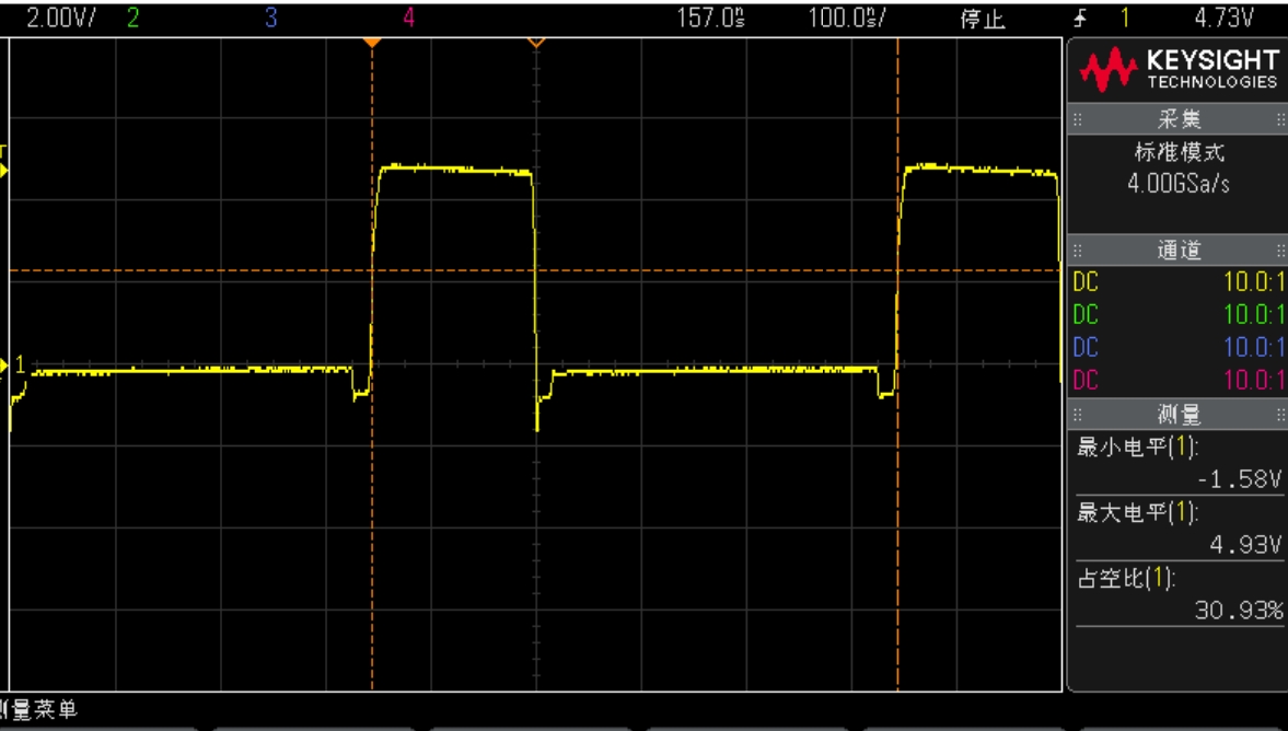
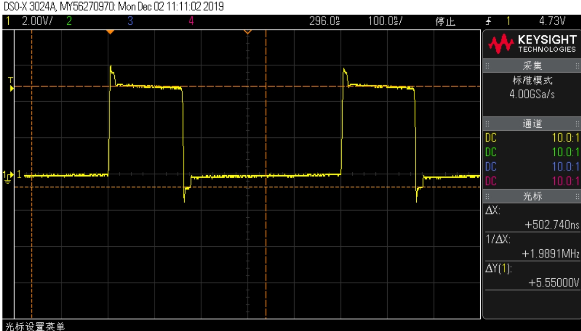
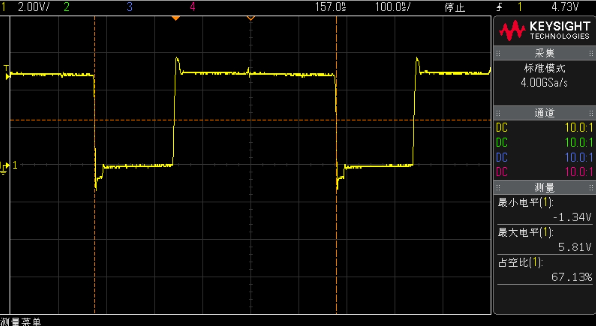
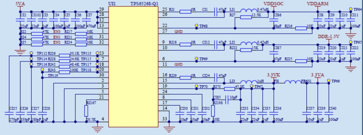
My customer use the TPS65268-Q1 and found that the SW pin negative pulse is very big.
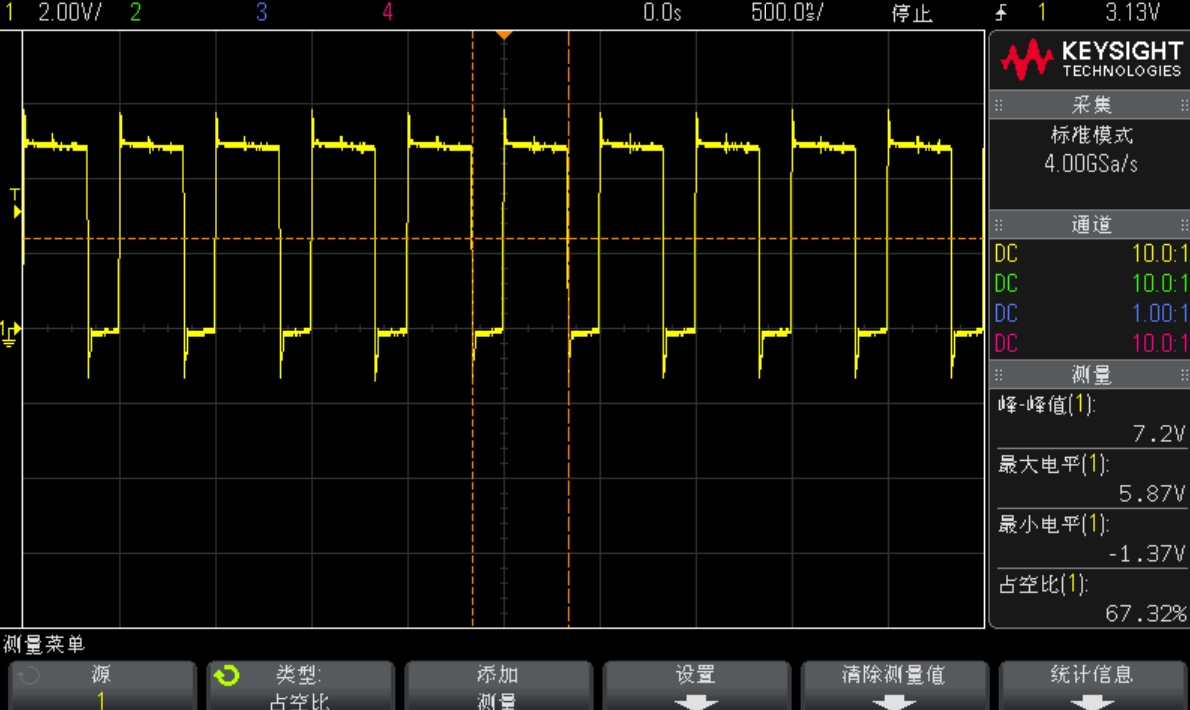
1)DDR=1.5V
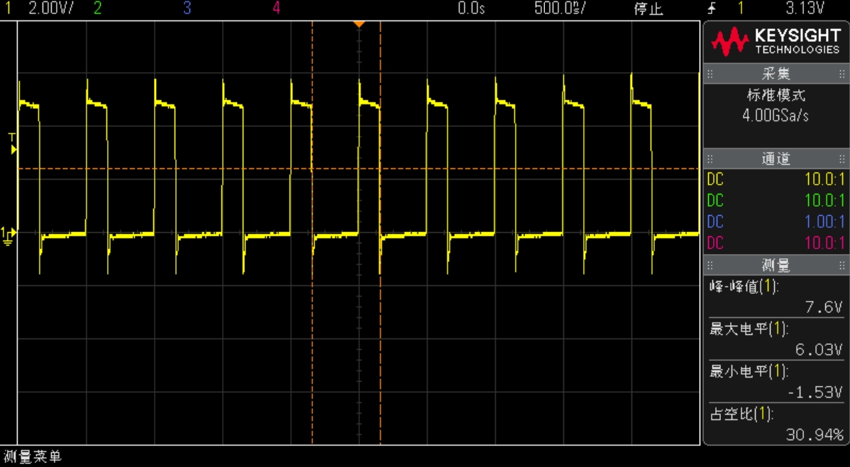
2)VDDARM-1.37V
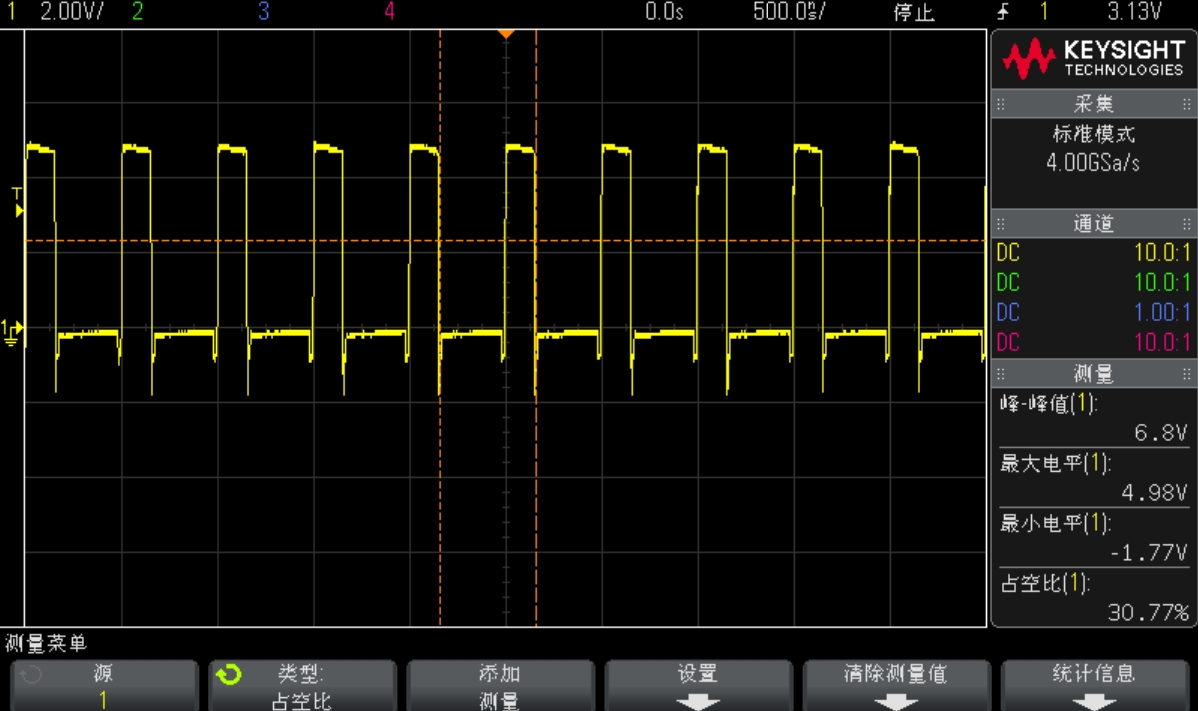
3)3.3VK
At present, no obvious problems have been found in the schematic diagram.
In layout, Vin and input capacitor are placed in the bottom layer; inductance and output capacitor are placed in the top layer. Input power loop is long, and it may be one of the reasons.
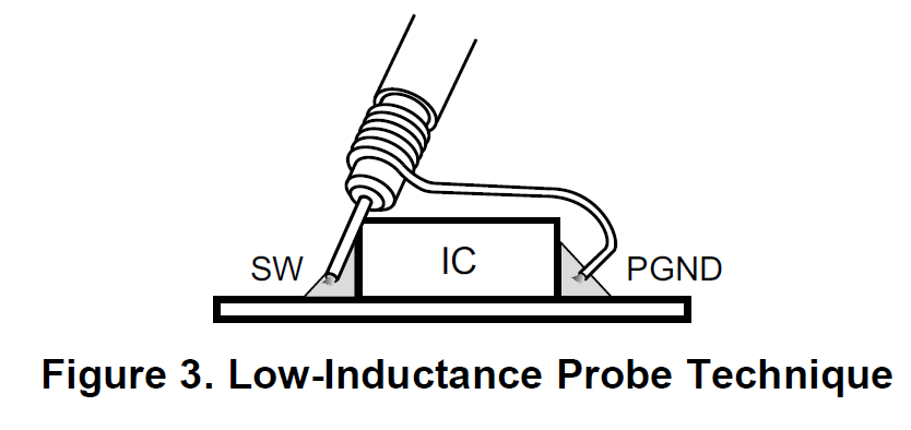
In addition, when adding RC to the ground (10R+1nF) in SW PIN , and no significant improvement was found.
Please help to confirm the problem, thank you!