


Hi Friends;
I have a problem about BQ40Z60 can't charge ;can you help me resolve?
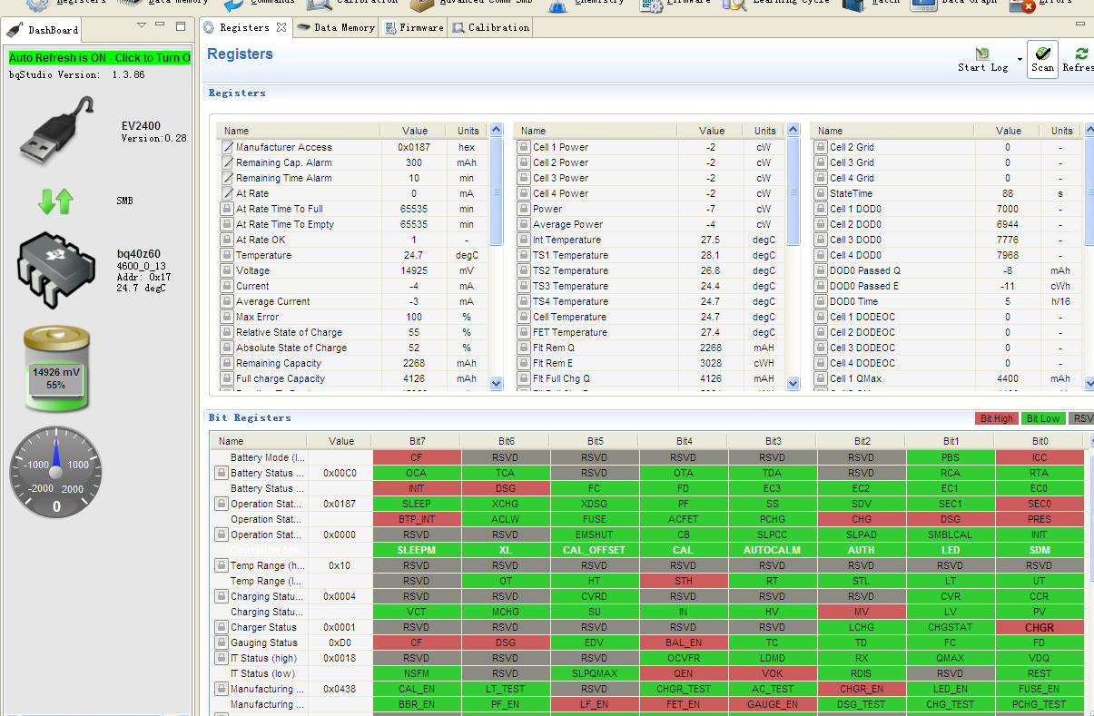
After the circuit is connected, the data is written, and the connection to the power supply 18-20v charging fails all the time.This is a four-string battery.
CHGR is always repeatedly setting the position clear. Attached are two GG files I tested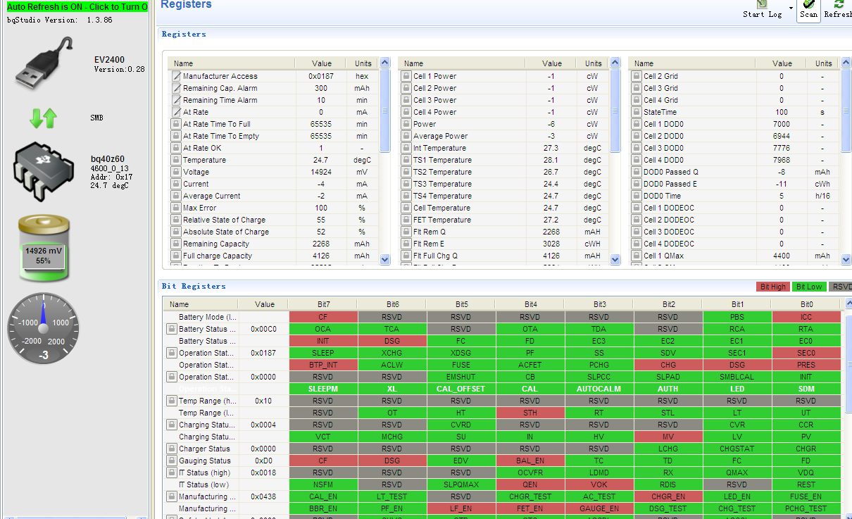
| * Texas Instruments Data Flash File | ||||
| * File created Mon Nov 25 20:39:53 2019 | ||||
| * | ||||
| * Device Number 4600 | ||||
| * Firmware Version 0.13 | ||||
| * Build Number 19 | ||||
| * Order Number 0 | ||||
| * | ||||
| * bqz Device Number 4600 | ||||
| * bqz Firmware Version 0.13 | ||||
| * bqz Build Number 19 | ||||
| * | ||||
| * Field Order: Class name | Subclass name | Parameter name | Parameter Value | Display Units |
| Calibration | Voltage | Cell Gain | 12101 | - |
| Calibration | Voltage | Pack Gain | 49669 | - |
| Calibration | Voltage | BAT Gain | 48936 | - |
| Calibration | Current | CC Gain | 9.876 | mOhm |
| Calibration | Current | Capacity Gain | 9.878 | mOhm |
| Calibration | Current Offset | CC Offset | 0 | - |
| Calibration | Current Offset | Coulomb Counter Offset Samples | 64 | - |
| Calibration | Current Offset | Board Offset | 0 | - |
| Calibration | Current Offset | CC Auto Config | 7 | hex |
| Calibration | Current Offset | CC Auto Offset | 33 | - |
| Calibration | Temperature | Internal Temp Offset | 0 | degC |
| Calibration | Temperature | External1 Temp Offset | 0 | degC |
| Calibration | Temperature | External2 Temp Offset | 0 | degC |
| Calibration | Temperature | External3 Temp Offset | 0 | degC |
| Calibration | Temperature | External4 Temp Offset | 0 | degC |
| Calibration | Internal Temp Model | Int Gain | -12143 | - |
| Calibration | Internal Temp Model | Int base offset | 6232 | - |
| Calibration | Internal Temp Model | Int Minimum AD | 0 | - |
| Calibration | Internal Temp Model | Int Maximum Temp | 6232 | 0.1degK |
| Calibration | Cell Temperature Model | Coeff a1 | -11130 | - |
| Calibration | Cell Temperature Model | Coeff a2 | 19142 | - |
| Calibration | Cell Temperature Model | Coeff a3 | -19262 | - |
| Calibration | Cell Temperature Model | Coeff a4 | 28203 | - |
| Calibration | Cell Temperature Model | Coeff a5 | 892 | - |
| Calibration | Cell Temperature Model | Coeff b1 | 328 | - |
| Calibration | Cell Temperature Model | Coeff b2 | -605 | - |
| Calibration | Cell Temperature Model | Coeff b3 | -2443 | - |
| Calibration | Cell Temperature Model | Coeff b4 | 4696 | - |
| Calibration | Cell Temperature Model | Rc0 | 11703 | - |
| Calibration | Cell Temperature Model | Adc0 | 11703 | - |
| Calibration | Cell Temperature Model | Rpad | 0 | - |
| Calibration | Cell Temperature Model | Rint | 0 | - |
| Calibration | Fet Temperature Model | Coeff a1 | -11130 | - |
| Calibration | Fet Temperature Model | Coeff a2 | 19142 | - |
| Calibration | Fet Temperature Model | Coeff a3 | -19262 | - |
| Calibration | Fet Temperature Model | Coeff a4 | 28203 | - |
| Calibration | Fet Temperature Model | Coeff a5 | 892 | - |
| Calibration | Fet Temperature Model | Coeff b1 | 328 | - |
| Calibration | Fet Temperature Model | Coeff b2 | -605 | - |
| Calibration | Fet Temperature Model | Coeff b3 | -2443 | - |
| Calibration | Fet Temperature Model | Coeff b4 | 4696 | - |
| Calibration | Fet Temperature Model | Rc0 | 11703 | - |
| Calibration | Fet Temperature Model | Adc0 | 11703 | - |
| Calibration | Fet Temperature Model | Rpad | 0 | - |
| Calibration | Fet Temperature Model | Rint | 0 | - |
| Calibration | Filter | Cell Voltage 1 | 145 | - |
| Calibration | Filter | Cell Voltage 2 | 145 | - |
| Calibration | Filter | Cell Voltage 3 | 145 | - |
| Calibration | Filter | Cell Voltage 4 | 145 | - |
| Calibration | Filter | Pack Voltage Out | 10 | - |
| Calibration | Filter | Direct Battery Voltage | 10 | - |
| Calibration | Filter | Summed Battery Voltage | 145 | - |
| Calibration | Filter | Cell Temperature | 145 | - |
| Calibration | Filter | FET Temperature | 145 | - |
| Calibration | Current Deadband | Deadband | 3 | mA |
| Calibration | Current Deadband | Coulomb Counter Deadband | 9 | 116nV |
| Settings | Protection | Protection Configuration | 0 | hex |
| Settings | Protection | Enabled Protections A | ff | hex |
| Settings | Protection | Enabled Protections B | 7f | hex |
| Settings | Protection | Enabled Protections C | fd | hex |
| Settings | Protection | Enabled Protections D | 2f | hex |
| Settings | Permanent Failure | Enabled PF A | 0 | hex |
| Settings | Permanent Failure | Enabled PF B | 0 | hex |
| Settings | Permanent Failure | Enabled PF C | 0 | hex |
| Settings | Permanent Failure | Enabled PF D | 0 | hex |
| Settings | Configuration | Charging Configuration | 0 | hex |
| Settings | Configuration | Temperature Enable | 6 | hex |
| Settings | Configuration | Temperature Mode | 0 | hex |
| Settings | Configuration | DA Configuration | 17 | hex |
| Settings | Configuration | FET Options | 24 | hex |
| Settings | Configuration | Sbs Gauging Configuration | 4 | hex |
| Settings | Configuration | Sbs Configuration | 20 | hex |
| Settings | Configuration | Power Config | 0 | hex |
| Settings | Configuration | IO Config | 0 | hex |
| Settings | Configuration | LED Configuration | 0 | hex |
| Settings | Configuration | SOC Flag Config A | 0c8c | hex |
| Settings | Configuration | SOC Flag Config B | 8c | hex |
| Settings | Configuration | Balancing Configuration | 1 | hex |
| Settings | Configuration | IT Gauging Configuration | d4fe | hex |
| Settings | AFE | AFE Protection Control | 70 | hex |
| Settings | AFE | ZVCHG Exit Threshold | 2200 | mV |
| Settings | Fuse | PF Fuse A | 0 | hex |
| Settings | Fuse | PF Fuse B | 0 | hex |
| Settings | Fuse | PF Fuse C | 0 | hex |
| Settings | Fuse | PF Fuse D | 0 | hex |
| Settings | Fuse | Min Blow Fuse Voltage | 3500 | mV |
| Settings | Fuse | Fuse Blow Timeout | 30 | s |
| Settings | BTP | Init Discharge Set | 150 | mAH |
| Settings | BTP | Init Charge Set | 175 | mAH |
| Settings | Manufacturing | Mfg Status init | 438 | hex |
| Protections | CUV | Threshold | 2500 | mV |
| Protections | CUV | Delay | 2 | s |
| Protections | CUV | Recovery | 3000 | mV |
| Protections | CUVC | Threshold | 2400 | mV |
| Protections | CUVC | Delay | 2 | s |
| Protections | CUVC | Recovery | 3000 | mV |
| Protections | COV | Threshold Low Temp | 4300 | mV |
| Protections | COV | Threshold Standard Temp | 4300 | mV |
| Protections | COV | Threshold High Temp | 4300 | mV |
| Protections | COV | Threshold Rec Temp | 4300 | mV |
| Protections | COV | Delay | 2 | s |
| Protections | COV | Recovery Low Temp | 4100 | mV |
| Protections | COV | Recovery Standard Temp | 4100 | mV |
| Protections | COV | Recovery High Temp | 4100 | mV |
| Protections | COV | Recovery Rec Temp | 4100 | mV |
| Protections | ACOV | Threshold | 24000 | mV |
| Protections | ACOV | Recovery | 22000 | mV |
| Protections | OCC1 | Threshold | 3000 | mA |
| Protections | OCC1 | Delay | 2 | s |
| Protections | OCC2 | Threshold | 5000 | mA |
| Protections | OCC2 | Delay | 1 | s |
| Protections | OCC | Recovery Threshold | 0 | mA |
| Protections | OCC | Recovery Delay | 10 | s |
| Protections | OCD1 | Threshold | -3000 | mA |
| Protections | OCD1 | Delay | 4 | s |
| Protections | OCD2 | Threshold | -5000 | mA |
| Protections | OCD2 | Delay | 2 | s |
| Protections | OCD | Recovery Threshold | 0 | mA |
| Protections | OCD | Recovery Delay | 10 | s |
| Protections | AOLD | Latch Limit | 0 | - |
| Protections | AOLD | Counter Dec Delay | 10 | s |
| Protections | AOLD | Recovery | 5 | s |
| Protections | AOLD | Reset | 15 | s |
| Protections | AOLD | Threshold | ff | hex |
| Protections | ASCC | Latch Limit | 0 | - |
| Protections | ASCC | Counter Dec Delay | 10 | s |
| Protections | ASCC | Recovery | 5 | s |
| Protections | ASCC | Reset | 15 | s |
| Protections | ASCC | Threshold | 77 | hex |
| Protections | ASCD | Latch Limit | 0 | - |
| Protections | ASCD | Counter Dec Delay | 10 | s |
| Protections | ASCD | Recovery | 5 | s |
| Protections | ASCD | Reset | 15 | s |
| Protections | ASCD | Threshold 1 | 77 | hex |
| Protections | ASCD | Threshold 2 | e7 | hex |
| Protections | OTC | Threshold | 50 | 1degC |
| Protections | OTC | Delay | 2 | s |
| Protections | OTC | Recovery | 45 | 1degC |
| Protections | OTD | Threshold | 60 | 1degC |
| Protections | OTD | Delay | 2 | s |
| Protections | OTD | Recovery | 55 | 1degC |
| Protections | OTF | Threshold | 80 | 1degC |
| Protections | OTF | Delay | 2 | s |
| Protections | OTF | Recovery | 65 | 1degC |
| Protections | UTC | Threshold | 0 | 1degC |
| Protections | UTC | Delay | 2 | s |
| Protections | UTC | Recovery | 5 | 1degC |
| Protections | UTD | Threshold | -20 | 1degC |
| Protections | UTD | Delay | 2 | s |
| Protections | UTD | Recovery | -15 | 1degC |
| Protections | COT | Recovery Delay | 5 | s |
| Protections | HWD | Delay | 10 | s |
| Protections | PTO | Charge Threshold | 2000 | mA |
| Protections | PTO | Suspend Threshold | 1800 | mA |
| Protections | PTO | Delay | 1800 | s |
| Protections | PTO | Reset | 2 | mAh |
| Protections | CTO | Charge Threshold | 2500 | mA |
| Protections | CTO | Suspend Threshold | 2000 | mA |
| Protections | CTO | Delay | 54000 | s |
| Protections | CTO | Reset | 2 | mAh |
| Protections | OC | Threshold | 300 | mAh |
| Protections | OC | Recovery | 2 | mAh |
| Protections | OC | RSOC Recovery | 90 | % |
| Protections | CHGV | Threshold | 500 | mV |
| Protections | CHGV | Delay | 30 | s |
| Protections | CHGV | Recovery | -500 | mV |
| Protections | CHGC | Threshold | 1000 | mA |
| Protections | CHGC | Delay | 8 | s |
| Protections | CHGC | Recovery Threshold | 100 | mA |
| Protections | CHGC | Recovery Delay | 2 | s |
| Protections | PCHGC | Threshold | 50 | mA |
| Protections | PCHGC | Delay | 2 | s |
| Protections | PCHGC | Recovery Threshold | 10 | mA |
| Protections | PCHGC | Recovery Delay | 2 | s |
| Permanent Fail | SUV | Threshold | 2200 | mV |
| Permanent Fail | SUV | Delay | 5 | s |
| Permanent Fail | SOV | Threshold | 4500 | mV |
| Permanent Fail | SOV | Delay | 5 | s |
| Permanent Fail | SOCC | Threshold | 10000 | mA |
| Permanent Fail | SOCC | Delay | 5 | s |
| Permanent Fail | SOCD | Threshold | -10000 | mA |
| Permanent Fail | SOCD | Delay | 5 | s |
| Permanent Fail | SOT | Threshold | 65 | 1degC |
| Permanent Fail | SOT | Delay | 5 | s |
| Permanent Fail | SOTF | Threshold | 100 | 1degC |
| Permanent Fail | SOTF | Delay | 5 | s |
| Permanent Fail | Open Thermistor | Threshold | -50 | 1degC |
| Permanent Fail | Open Thermistor | Delay | 5 | s |
| Permanent Fail | Open Thermistor | Fet Delta | 20 | 1degC |
| Permanent Fail | Open Thermistor | Cell Delta | 20 | 1degC |
| Permanent Fail | QIM | Delta Threshold | 15 | % |
| Permanent Fail | QIM | Delay | 2 | updates |
| Permanent Fail | CB | Max Threshold | 240 | h |
| Permanent Fail | CB | Delta Threshold | 40 | h |
| Permanent Fail | CB | Delay | 2 | cycles |
| Permanent Fail | VIMR | Check Voltage | 3500 | mV |
| Permanent Fail | VIMR | Check Current | 10 | mA |
| Permanent Fail | VIMR | Delta Threshold | 500 | mV |
| Permanent Fail | VIMR | Delta Delay | 5 | s |
| Permanent Fail | VIMR | Duration | 100 | s |
| Permanent Fail | VIMA | Check Voltage | 3700 | mV |
| Permanent Fail | VIMA | Check Current | 50 | mA |
| Permanent Fail | VIMA | Delta Threshold | 200 | mV |
| Permanent Fail | VIMA | Delay | 5 | s |
| Permanent Fail | IMP | Delta Threshold | 300 | % |
| Permanent Fail | IMP | Max Threshold | 400 | % |
| Permanent Fail | IMP | Ra Update Counts | 2 | counts |
| Permanent Fail | CD | Threshold | 0 | mAh |
| Permanent Fail | CD | Delay | 2 | cycles |
| Permanent Fail | CFET | OFF Threshold | 5 | mA |
| Permanent Fail | CFET | OFF Delay | 5 | s |
| Permanent Fail | DFET | OFF Threshold | -50 | mA |
| Permanent Fail | DFET | OFF Delay | 5 | s |
| Permanent Fail | FUSE | Threshold | 5 | mA |
| Permanent Fail | FUSE | Delay | 5 | s |
| Permanent Fail | AFER | Threshold | 100 | - |
| Permanent Fail | AFER | Delay Period | 2 | s |
| Permanent Fail | AFER | Compare Period | 5 | s |
| Permanent Fail | AFEC | Threshold | 100 | - |
| Permanent Fail | AFEC | Delay Period | 5 | s |
| Permanent Fail | 2LVL | Delay | 5 | s |
| Permanent Fail | OPNCELL | Threshold | 5000 | mV |
| Permanent Fail | OPNCELL | Delay | 5 | s |
| Advanced Charge Algorithm | Charger | Minimum Voltage Output | 8644 | mV |
| Advanced Charge Algorithm | Charger | Voltage Resolution | 34 | mV |
| Advanced Charge Algorithm | Charger | LCHG Current Resolution | 8 | mA |
| Advanced Charge Algorithm | Charger | Current Resolution | 39 | mA |
| Advanced Charge Algorithm | Charger | Max Current Register | 255 | - |
| Advanced Charge Algorithm | Charger | Vacp Hysteresis | 0 | mV |
| Advanced Charge Algorithm | Temperature Ranges | T1 Temp | 0 | degC |
| Advanced Charge Algorithm | Temperature Ranges | T2 Temp | 12 | degC |
| Advanced Charge Algorithm | Temperature Ranges | T5 Temp | 20 | degC |
| Advanced Charge Algorithm | Temperature Ranges | T6 Temp | 25 | degC |
| Advanced Charge Algorithm | Temperature Ranges | T3 Temp | 40 | degC |
| Advanced Charge Algorithm | Temperature Ranges | T4 Temp | 55 | degC |
| Advanced Charge Algorithm | Temperature Ranges | Hysteresis Temp | 1 | degC |
| Advanced Charge Algorithm | Low Temp Charging | Voltage | 4000 | mV |
| Advanced Charge Algorithm | Low Temp Charging | Current Low | 400 | mA |
| Advanced Charge Algorithm | Low Temp Charging | Current Med | 400 | mA |
| Advanced Charge Algorithm | Low Temp Charging | Current High | 400 | mA |
| Advanced Charge Algorithm | Standard Temp Charging | Voltage | 4200 | mV |
| Advanced Charge Algorithm | Standard Temp Charging | Current Low | 1000 | mA |
| Advanced Charge Algorithm | Standard Temp Charging | Current Med | 1000 | mA |
| Advanced Charge Algorithm | Standard Temp Charging | Current High | 1000 | mA |
| Advanced Charge Algorithm | High Temp Charging | Voltage | 4000 | mV |
| Advanced Charge Algorithm | High Temp Charging | Current Low | 500 | mA |
| Advanced Charge Algorithm | High Temp Charging | Current Med | 500 | mA |
| Advanced Charge Algorithm | High Temp Charging | Current High | 500 | mA |
| Advanced Charge Algorithm | Rec Temp Charging | Voltage | 4200 | mV |
| Advanced Charge Algorithm | Rec Temp Charging | Current Low | 1000 | mA |
| Advanced Charge Algorithm | Rec Temp Charging | Current Med | 1000 | mA |
| Advanced Charge Algorithm | Rec Temp Charging | Current High | 1000 | mA |
| Advanced Charge Algorithm | Pre-Charging | Current | 200 | mA |
| Advanced Charge Algorithm | Maintenance Charging | Current | 44 | mA |
| Advanced Charge Algorithm | Voltage Range | Precharge Start Voltage | 2500 | mV |
| Advanced Charge Algorithm | Voltage Range | Charging Voltage Low | 2900 | mV |
| Advanced Charge Algorithm | Voltage Range | Charging Voltage Med | 3600 | mV |
| Advanced Charge Algorithm | Voltage Range | Charging Voltage High | 4000 | mV |
| Advanced Charge Algorithm | Voltage Range | Charging Voltage Hysteresis | 0 | mV |
| Advanced Charge Algorithm | Termination Config | Charge Term Taper Current | 250 | mA |
| Advanced Charge Algorithm | Termination Config | Charge Term Voltage | 75 | mV |
| Advanced Charge Algorithm | Charging Rate of Change | Current Rate | 1 | steps |
| Advanced Charge Algorithm | Charging Rate of Change | Voltage Rate | 1 | steps |
| Advanced Charge Algorithm | Cell Balancing Config | Bal Time/mAh Cell 1 | 367 | s/mAh |
| Advanced Charge Algorithm | Cell Balancing Config | Bal Time/mAh Cell 2-4 | 514 | s/mAh |
| Advanced Charge Algorithm | Cell Balancing Config | Min Start Balance Delta | 3 | mV |
| Advanced Charge Algorithm | Cell Balancing Config | Relax Balance Interval | 18000 | s |
| Advanced Charge Algorithm | Cell Balancing Config | Min Rsoc for Balancing | 80 | % |
| Gas Gauging | Current Thresholds | Dsg Current Threshold | 100 | mA |
| Gas Gauging | Current Thresholds | Chg Current Threshold | 50 | mA |
| Gas Gauging | Current Thresholds | Quit Current | 10 | mA |
| Gas Gauging | Current Thresholds | Dsg Relax Time | 1 | s |
| Gas Gauging | Current Thresholds | Chg Relax Time | 60 | s |
| Gas Gauging | Current Thresholds | Dsg Body Diode Protect Threshold | 100 | mA |
| Gas Gauging | Current Thresholds | Chg Body Diode Threshold | 100 | mA |
| Gas Gauging | Design | Design Capacity mAh | 3300 | mAh |
| Gas Gauging | Design | Design Capacity cWh | 4884 | cWh |
| Gas Gauging | Design | Design Voltage | 14800 | mV |
| Gas Gauging | Cycle | Cycle Count Percentage | 90 | % |
| Gas Gauging | FD | Set Voltage Threshold | 3000 | mV |
| Gas Gauging | FD | Clear Voltage Threshold | 3100 | mV |
| Gas Gauging | FD | Set % RSOC Threshold | 0 | % |
| Gas Gauging | FD | Clear % RSOC Threshold | 5 | % |
| Gas Gauging | FC | Set Voltage Threshold | 4200 | mV |
| Gas Gauging | FC | Clear Voltage Threshold | 4100 | mV |
| Gas Gauging | FC | Set % RSOC Threshold | 100 | % |
| Gas Gauging | FC | Clear % RSOC Threshold | 95 | % |
| Gas Gauging | TD | Set Voltage Threshold | 3200 | mV |
| Gas Gauging | TD | Clear Voltage Threshold | 3300 | mV |
| Gas Gauging | TD | Set % RSOC Threshold | 6 | % |
| Gas Gauging | TD | Clear % RSOC Treshold | 8 | % |
| Gas Gauging | TC | Set Voltage Threshold | 4200 | mV |
| Gas Gauging | TC | Clear Voltage Threshold | 4100 | mV |
| Gas Gauging | TC | Set % RSOC Threshold | 100 | % |
| Gas Gauging | TC | Clear % RSOC Threshold | 95 | % |
| Gas Gauging | State | Cycle Count | 0 | - |
| Gas Gauging | State | Qmax Cell 1 | 3300 | mAh |
| Gas Gauging | State | Qmax Cell 2 | 3300 | mAh |
| Gas Gauging | State | Qmax Cell 3 | 3300 | mAh |
| Gas Gauging | State | Qmax Cell 4 | 3300 | mAh |
| Gas Gauging | State | Qmax Pack | 3300 | mAh |
| Gas Gauging | State | Qmax Cycle Count | 0 | - |
| Gas Gauging | State | Update Status | 4 | - |
| Gas Gauging | State | Cell 1 Chg Voltage at EoC | 4200 | mV |
| Gas Gauging | State | Cell 2 Chg Voltage at EoC | 4200 | mV |
| Gas Gauging | State | Cell 3 Chg Voltage at EoC | 4200 | mV |
| Gas Gauging | State | Cell 4 Chg Voltage at EoC | 4200 | mV |
| Gas Gauging | State | Current at EoC | 250 | mA |
| Gas Gauging | State | Avg I Last Run | -2000 | mA |
| Gas Gauging | State | Avg P Last Run | -3022 | cW |
| Gas Gauging | State | Delta Voltage | 0 | mV |
| Gas Gauging | State | Temp k | 1 | degC/256mW |
| Gas Gauging | State | Temp a | 1000 | - |
| Gas Gauging | State | Max Avg I Last Run | -2000 | mA |
| Gas Gauging | State | Max Avg P Last Run | -3022 | cW |
| Gas Gauging | IT Cfg | Load Select | 7 | - |
| Gas Gauging | IT Cfg | Load Mode | 0 | - |
| Gas Gauging | IT Cfg | Design Resistance | 42 | mOhms |
| Gas Gauging | IT Cfg | User Rate-mA | 0 | mA |
| Gas Gauging | IT Cfg | User Rate-cW | 0 | cW |
| Gas Gauging | IT Cfg | Reserve Cap-mAh | 0 | mAh |
| Gas Gauging | IT Cfg | Reserve Cap-cWh | 0 | cWh |
| Gas Gauging | IT Cfg | Pack Resistance | 30 | mOhms |
| Gas Gauging | IT Cfg | System Resistance | 0 | mOhms |
| Gas Gauging | IT Cfg | Ra Filter | 50 | % |
| Gas Gauging | IT Cfg | Ra Max Delta | 15 | % |
| Gas Gauging | IT Cfg | Reference Grid | 4 | - |
| Gas Gauging | IT Cfg | Resistance Parameter Filter | 65142 | - |
| Gas Gauging | IT Cfg | Near EDV Ra Param Filter | 59220 | - |
| Gas Gauging | IT Cfg | Qmax Delta | 5 | % |
| Gas Gauging | IT Cfg | Qmax Upper Bound | 130 | % |
| Gas Gauging | IT Cfg | Term Voltage | 9000 | mV |
| Gas Gauging | IT Cfg | Term V Hold Time | 1 | s |
| Gas Gauging | IT Cfg | Term Voltage Delta | 300 | mV |
| Gas Gauging | IT Cfg | Term Min Cell V | 2800 | mV |
| Gas Gauging | IT Cfg | Voltage Consistency Delta | 300 | mV |
| Gas Gauging | IT Cfg | Fast Scale Start SOC | 10 | % |
| Gas Gauging | Smoothing | Smooth Relax Time | 1000 | s |
| Gas Gauging | Condition Flag | Max Error Limit | 100 | % |
| Gas Gauging | Max Error | Time Cycle Equivalent | 24 | h |
| Gas Gauging | Max Error | Cycle Delta | 0.05 | % |
| Gas Gauging | SoH | SoH Load Rate | 5 | hour Rate |
| Gas Gauging | Turbo Cfg | Min Turbo Power | 0 | cW |
| Gas Gauging | Turbo Cfg | Max C Rate | -4 | C |
| Gas Gauging | Turbo Cfg | High Frequency Resistance | 61 | mOhms |
| Gas Gauging | Turbo Cfg | Reserve Energy % | 0 | % |
| Power | Power | Valid Update Voltage | 3500 | mV |
| Power | Shutdown | Shutdown Voltage | 1750 | mV |
| Power | Shutdown | Shutdown Time | 10 | s |
| Power | Shutdown | PF Shutdown Voltage | 1750 | mV |
| Power | Shutdown | PF Shutdown Time | 10 | s |
| Power | Shutdown | Charger Present Threshold | 3000 | mV |
| Power | Sleep | Sleep Current | 10 | mA |
| Power | Sleep | Bus Timeout | 5 | s |
| Power | Sleep | Voltage Time | 5 | s |
| Power | Sleep | Current Time | 20 | s |
| Power | Sleep | Wake Comparitor | 0 | hex |
| Power | Ship | FET Off Time | 10 | s |
| Power | Ship | Delay | 20 | s |
| Power | Ship | Auto Ship Time | 1440 | min |
| Power | Power Off | Debounce | 4 | 250ms |
| Power | Power Off | Timeout | 30 | min |
| Power | Manual FET Control | MFC Delay | 60 | s |
| PF Status | Device Status Data | Safety Alert A | 0 | hex |
| PF Status | Device Status Data | Safety Status A | 0 | hex |
| PF Status | Device Status Data | Safety Alert B | 0 | hex |
| PF Status | Device Status Data | Safety Status B | 0 | hex |
| PF Status | Device Status Data | Safety Alert C | 0 | hex |
| PF Status | Device Status Data | Safety Status C | 0 | hex |
| PF Status | Device Status Data | Safety Alert D | 0 | hex |
| PF Status | Device Status Data | Safety Status D | 0 | hex |
| PF Status | Device Status Data | PF Alert A | 0 | hex |
| PF Status | Device Status Data | PF Status A | 0 | hex |
| PF Status | Device Status Data | PF Alert B | 0 | hex |
| PF Status | Device Status Data | PF Status B | 0 | hex |
| PF Status | Device Status Data | PF Alert C | 0 | hex |
| PF Status | Device Status Data | PF Status C | 0 | hex |
| PF Status | Device Status Data | PF Alert D | 0 | hex |
| PF Status | Device Status Data | PF Status D | 0 | hex |
| PF Status | Device Status Data | Fuse Flag | 0 | hex |
| PF Status | Device Status Data | Operation Status A | 0 | hex |
| PF Status | Device Status Data | Operation Status B | 0 | hex |
| PF Status | Device Status Data | Temp Range | 0 | hex |
| PF Status | Device Status Data | Charging Status A | 0 | hex |
| PF Status | Device Status Data | Charging Status B | 0 | hex |
| PF Status | Device Status Data | Charger Status | 0 | hex |
| PF Status | Device Status Data | Gauging Status | 0 | hex |
| PF Status | Device Status Data | IT Status | 0 | hex |
| PF Status | Device Voltage Data | Cell 1 Voltage | 0 | mV |
| PF Status | Device Voltage Data | Cell 2 Voltage | 0 | mV |
| PF Status | Device Voltage Data | Cell 3 Voltage | 0 | mV |
| PF Status | Device Voltage Data | Cell 4 Voltage | 0 | mV |
| PF Status | Device Voltage Data | Battery Direct Voltage | 0 | mV |
| PF Status | Device Voltage Data | Pack Voltage | 0 | mV |
| PF Status | Device Current Data | Current | 0 | mA |
| PF Status | Device Temperature Data | Internal Temperature | -273.2 | degC |
| PF Status | Device Temperature Data | External 1 Temperature | -273.2 | degC |
| PF Status | Device Temperature Data | External 2 Temperature | -273.2 | degC |
| PF Status | Device Temperature Data | External 3 Temperature | -273.2 | degC |
| PF Status | Device Temperature Data | External 4 Temperature | -273.2 | degC |
| PF Status | Device Gauging Data | Cell 1 Dod0 | 0 | - |
| PF Status | Device Gauging Data | Cell 2 Dod0 | 0 | - |
| PF Status | Device Gauging Data | Cell 3 Dod0 | 0 | - |
| PF Status | Device Gauging Data | Cell 4 Dod0 | 0 | - |
| PF Status | Device Gauging Data | Passed Charge | 0 | mAh |
| PF Status | AFE Regs | AFE Interrupt Status | 0 | hex |
| PF Status | AFE Regs | AFE FET Status | 0 | hex |
| PF Status | AFE Regs | AFE RXIN | 0 | hex |
| PF Status | AFE Regs | AFE Latch Status | 0 | hex |
| PF Status | AFE Regs | AFE Interrupt Enable | 0 | hex |
| PF Status | AFE Regs | AFE FET Control | 0 | hex |
| PF Status | AFE Regs | AFE RXIEN | 0 | hex |
| PF Status | AFE Regs | AFE RLOUT | 0 | hex |
| PF Status | AFE Regs | AFE RHOUT | 0 | hex |
| PF Status | AFE Regs | AFE RHINT | 0 | hex |
| PF Status | AFE Regs | AFE Cell Balance | 0 | hex |
| PF Status | AFE Regs | AFE AD/CC Control | 0 | hex |
| PF Status | AFE Regs | AFE ADC Mux | 0 | hex |
| PF Status | AFE Regs | AFE LED Output | 0 | hex |
| PF Status | AFE Regs | AFE State Control | 0 | hex |
| PF Status | AFE Regs | AFE LED/Wake Control | 0 | hex |
| PF Status | AFE Regs | AFE Protection Control | 0 | hex |
| PF Status | AFE Regs | AFE OCD | 0 | hex |
| PF Status | AFE Regs | AFE SCC | 0 | hex |
| PF Status | AFE Regs | AFE SCD1 | 0 | hex |
| PF Status | AFE Regs | AFE SCD2 | 0 | hex |
| PF Status | AFE Regs | AFE Charger Lock | 0 | |
| PF Status | AFE Regs | AFE Charger Voltage | 0 | |
| PF Status | AFE Regs | AFE Charger Current | 0 | |
| System Data | Manufacturer Data | Manufacturer Info A Length | 32 | - |
| System Data | Manufacturer Data | Manufacturer Info Block A01 | 61 | Hex |
| System Data | Manufacturer Data | Manufacturer Info Block A02 | 62 | Hex |
| System Data | Manufacturer Data | Manufacturer Info Block A03 | 63 | Hex |
| System Data | Manufacturer Data | Manufacturer Info Block A04 | 64 | Hex |
| System Data | Manufacturer Data | Manufacturer Info Block A05 | 65 | Hex |
| System Data | Manufacturer Data | Manufacturer Info Block A06 | 66 | Hex |
| System Data | Manufacturer Data | Manufacturer Info Block A07 | 67 | Hex |
| System Data | Manufacturer Data | Manufacturer Info Block A08 | 68 | Hex |
| System Data | Manufacturer Data | Manufacturer Info Block A09 | 69 | Hex |
| System Data | Manufacturer Data | Manufacturer Info Block A10 | 6a | Hex |
| System Data | Manufacturer Data | Manufacturer Info Block A11 | 6b | Hex |
| System Data | Manufacturer Data | Manufacturer Info Block A12 | 6c | Hex |
| System Data | Manufacturer Data | Manufacturer Info Block A13 | 6d | Hex |
| System Data | Manufacturer Data | Manufacturer Info Block A14 | 6e | Hex |
| System Data | Manufacturer Data | Manufacturer Info Block A15 | 6f | Hex |
| System Data | Manufacturer Data | Manufacturer Info Block A16 | 70 | Hex |
| System Data | Manufacturer Data | Manufacturer Info Block A17 | 71 | Hex |
| System Data | Manufacturer Data | Manufacturer Info Block A18 | 72 | Hex |
| System Data | Manufacturer Data | Manufacturer Info Block A19 | 73 | Hex |
| System Data | Manufacturer Data | Manufacturer Info Block A20 | 74 | Hex |
| System Data | Manufacturer Data | Manufacturer Info Block A21 | 75 | Hex |
| System Data | Manufacturer Data | Manufacturer Info Block A22 | 76 | Hex |
| System Data | Manufacturer Data | Manufacturer Info Block A23 | 77 | Hex |
| System Data | Manufacturer Data | Manufacturer Info Block A24 | 7a | Hex |
| System Data | Manufacturer Data | Manufacturer Info Block A25 | 78 | Hex |
| System Data | Manufacturer Data | Manufacturer Info Block A26 | 79 | Hex |
| System Data | Manufacturer Data | Manufacturer Info Block A27 | 30 | Hex |
| System Data | Manufacturer Data | Manufacturer Info Block A28 | 31 | Hex |
| System Data | Manufacturer Data | Manufacturer Info Block A29 | 32 | Hex |
| System Data | Manufacturer Data | Manufacturer Info Block A30 | 33 | Hex |
| System Data | Manufacturer Data | Manufacturer Info Block A31 | 34 | Hex |
| System Data | Manufacturer Data | Manufacturer Info Block A32 | 35 | Hex |
| System Data | Integrity | Static DF Signature | 0 | hex |
| System Data | Integrity | Static Chem DF Signature | 3d63 | hex |
| System Data | Integrity | All DF Signature | 0 | hex |
| SBS Configuration | Data | Remaining AH Cap. Alarm | 300 | mAh |
| SBS Configuration | Data | Remaining WH Cap. Alarm | 432 | cWh |
| SBS Configuration | Data | Remaining Time Alarm | 10 | min |
| SBS Configuration | Data | Initial Battery Mode | 81 | hex |
| SBS Configuration | Data | Specification Information | 31 | hex |
| SBS Configuration | Data | Manufacture Date | ######## | date |
| SBS Configuration | Data | Serial Number | 1 | hex |
| SBS Configuration | Data | Manufacturer Name | H.B | - |
| SBS Configuration | Data | Device Name | bq40z60 | - |
| SBS Configuration | Data | Device Chemistry | LION | - |
| LED Support | LED Config | LED Delay | 100 | 488us |
| LED Support | LED Config | LED Hold Time | 4 | s |
| LED Support | LED Config | CHG Thresh 1 | 25 | % |
| LED Support | LED Config | CHG Thresh 2 | 50 | % |
| LED Support | LED Config | CHG Thresh 3 | 75 | % |
| LED Support | LED Config | CHG Thresh 4 | 100 | % |
| LED Support | LED Config | DSG Thresh 1 | 25 | % |
| LED Support | LED Config | DSG Thresh 2 | 50 | % |
| LED Support | LED Config | DSG Thresh 3 | 75 | % |
| LED Support | LED Config | DSG Thresh 4 | 100 | % |
| Black Box | Safety Status | 1st Status Status A | 0 | hex |
| Black Box | Safety Status | 1st Status Status B | 0 | hex |
| Black Box | Safety Status | 1st Safety Status C | 0 | hex |
| Black Box | Safety Status | 1st Safety Status D | 0 | hex |
| Black Box | Safety Status | 1st Time to Next Event | 0 | s |
| Black Box | Safety Status | 2nd Status Status A | 0 | hex |
| Black Box | Safety Status | 2nd Status Status B | 0 | hex |
| Black Box | Safety Status | 2nd Safety Status C | 0 | hex |
| Black Box | Safety Status | 2nd Safety Status D | 0 | hex |
| Black Box | Safety Status | 2nd Time to Next Event | 0 | s |
| Black Box | Safety Status | 3rd Status Status A | 0 | hex |
| Black Box | Safety Status | 3rd Status Status B | 0 | hex |
| Black Box | Safety Status | 3rd Safety Status C | 0 | hex |
| Black Box | Safety Status | 3rd Safety Status D | 0 | hex |
| Black Box | Safety Status | 3rd Time to Next Event | 0 | s |
| Black Box | PF Status | 1st PF Status A | 0 | hex |
| Black Box | PF Status | 1st PF Status B | 0 | hex |
| Black Box | PF Status | 1st PF Status C | 0 | hex |
| Black Box | PF Status | 1st PF Status D | 0 | hex |
| Black Box | PF Status | 1st Time to Next Event | 0 | s |
| Black Box | PF Status | 2nd PF Status A | 0 | hex |
| Black Box | PF Status | 2nd PF Status B | 0 | hex |
| Black Box | PF Status | 2nd PF Status C | 0 | hex |
| Black Box | PF Status | 2nd PF Status D | 0 | hex |
| Black Box | PF Status | 2nd Time to Next Event | 0 | s |
| Black Box | PF Status | 3rd PF Status A | 0 | hex |
| Black Box | PF Status | 3rd PF Status B | 0 | hex |
| Black Box | PF Status | 3rd PF Status C | 0 | hex |
| Black Box | PF Status | 3rd PF Status D | 0 | hex |
| Black Box | PF Status | 3rd Time to Next Event | 0 | s |
| Lifetimes | Voltage | Cell 1 Max Voltage | 0 | mV |
| Lifetimes | Voltage | Cell 2 Max Voltage | 0 | mV |
| Lifetimes | Voltage | Cell 3 Max Voltage | 0 | mV |
| Lifetimes | Voltage | Cell 4 Max Voltage | 0 | mV |
| Lifetimes | Voltage | Cell 1 Min Voltage | 32767 | mV |
| Lifetimes | Voltage | Cell 2 Min Voltage | 32767 | mV |
| Lifetimes | Voltage | Cell 3 Min Voltage | 32767 | mV |
| Lifetimes | Voltage | Cell 4 Min Voltage | 32767 | mV |
| Lifetimes | Voltage | Max Delta Cell Voltage | 0 | mV |
| Lifetimes | Current | Max Charge Current | 0 | mA |
| Lifetimes | Current | Max Discharge Current | 0 | mA |
| Lifetimes | Current | Max Avg Dsg Current | 0 | mA |
| Lifetimes | Current | Max Avg Dsg Power | 0 | cW |
| Lifetimes | Temperature | Max Temp Cell | -128 | degC |
| Lifetimes | Temperature | Min Temp Cell | 127 | degC |
| Lifetimes | Temperature | Max Delta Cell Temp | 0 | degC |
| Lifetimes | Temperature | Max Temp Int Sensor | -128 | degC |
| Lifetimes | Temperature | Min Temp Int Sensor | 127 | degC |
| Lifetimes | Temperature | Max Temp Fet | -128 | degC |
| Lifetimes | Safety Events | No Of COV Events | 0 | events |
| Lifetimes | Safety Events | Last COV Event | 0 | cycles |
| Lifetimes | Safety Events | No Of CUV Events | 0 | events |
| Lifetimes | Safety Events | Last CUV Event | 0 | cycles |
| Lifetimes | Safety Events | No Of OCD1 Events | 0 | events |
| Lifetimes | Safety Events | Last OCD1 Event | 0 | cycles |
| Lifetimes | Safety Events | No Of OCD2 Events | 0 | events |
| Lifetimes | Safety Events | Last OCD2 Event | 0 | cycles |
| Lifetimes | Safety Events | No Of OCC1 Events | 0 | events |
| Lifetimes | Safety Events | Last OCC1 Event | 0 | cycles |
| Lifetimes | Safety Events | No Of OCC2 Events | 0 | events |
| Lifetimes | Safety Events | Last OCC2 Event | 0 | cycles |
| Lifetimes | Safety Events | No Of AOLD Events | 0 | events |
| Lifetimes | Safety Events | Last AOLD Event | 0 | cycles |
| Lifetimes | Safety Events | No Of ASCD Events | 0 | events |
| Lifetimes | Safety Events | Last ASCD Event | 0 | cycles |
| Lifetimes | Safety Events | No Of ASCC Events | 0 | events |
| Lifetimes | Safety Events | Last ASCC Event | 0 | cycles |
| Lifetimes | Safety Events | No Of OTC Events | 0 | events |
| Lifetimes | Safety Events | Last OTC Event | 0 | cycles |
| Lifetimes | Safety Events | No Of OTD Events | 0 | events |
| Lifetimes | Safety Events | Last OTD Event | 0 | cycles |
| Lifetimes | Safety Events | No Of OTF Events | 0 | events |
| Lifetimes | Safety Events | Last OTF Event | 0 | cycles |
| Lifetimes | Charging Events | No Valid Charge Term | 0 | events |
| Lifetimes | Charging Events | Last Valid Charge Term | 0 | cycles |
| Lifetimes | Gauging Events | No Of Qmax Updates | 0 | events |
| Lifetimes | Gauging Events | Last Qmax Update | 0 | cycles |
| Lifetimes | Gauging Events | No Of Ra Updates | 0 | events |
| Lifetimes | Gauging Events | Last Ra Update | 0 | cycles |
| Lifetimes | Gauging Events | No Of Ra Disable | 0 | events |
| Lifetimes | Gauging Events | Last Ra Disable | 0 | cycles |
| Lifetimes | Power Events | No Of Shutdowns | 0 | events |
| Lifetimes | Cell Balancing | Cb Time Cell 1 | 0 | h |
| Lifetimes | Cell Balancing | Cb Time Cell 2 | 0 | h |
| Lifetimes | Cell Balancing | Cb Time Cell 3 | 0 | h |
| Lifetimes | Cell Balancing | Cb Time Cell 4 | 0 | h |
| Lifetimes | Time | Total Fw Runtime | 0 | h |
| Lifetimes | Time | Time Spent In UT | 0 | h |
| Lifetimes | Time | Time Spent In LT | 0 | h |
| Lifetimes | Time | Time Spent In STL | 0 | h |
| Lifetimes | Time | Time Spent In RT | 0 | h |
| Lifetimes | Time | Time Spent In STH | 0 | h |
| Lifetimes | Time | Time Spent In HT | 0 | h |
| Lifetimes | Time | Time Spent In OT | 0 | h |
| Ra Table | R_a0 | Cell0 R_a flag | ff55 | - |
| Ra Table | R_a0 | Cell0 R_a 0 | 97 | 2^-10ohm |
| Ra Table | R_a0 | Cell0 R_a 1 | 99 | 2^-10ohm |
| Ra Table | R_a0 | Cell0 R_a 2 | 121 | 2^-10ohm |
| Ra Table | R_a0 | Cell0 R_a 3 | 119 | 2^-10ohm |
| Ra Table | R_a0 | Cell0 R_a 4 | 94 | 2^-10ohm |
| Ra Table | R_a0 | Cell0 R_a 5 | 109 | 2^-10ohm |
| Ra Table | R_a0 | Cell0 R_a 6 | 111 | 2^-10ohm |
| Ra Table | R_a0 | Cell0 R_a 7 | 104 | 2^-10ohm |
| Ra Table | R_a0 | Cell0 R_a 8 | 156 | 2^-10ohm |
| Ra Table | R_a0 | Cell0 R_a 9 | 185 | 2^-10ohm |
| Ra Table | R_a0 | Cell0 R_a 10 | 355 | 2^-10ohm |
| Ra Table | R_a0 | Cell0 R_a 11 | 435 | 2^-10ohm |
| Ra Table | R_a0 | Cell0 R_a 12 | 582 | 2^-10ohm |
| Ra Table | R_a0 | Cell0 R_a 13 | 1256 | 2^-10ohm |
| Ra Table | R_a0 | Cell0 R_a 14 | 3036 | 2^-10ohm |
| Ra Table | R_a1 | Cell1 R_a flag | ff55 | - |
| Ra Table | R_a1 | Cell1 R_a 0 | 97 | 2^-10ohm |
| Ra Table | R_a1 | Cell1 R_a 1 | 99 | 2^-10ohm |
| Ra Table | R_a1 | Cell1 R_a 2 | 121 | 2^-10ohm |
| Ra Table | R_a1 | Cell1 R_a 3 | 119 | 2^-10ohm |
| Ra Table | R_a1 | Cell1 R_a 4 | 94 | 2^-10ohm |
| Ra Table | R_a1 | Cell1 R_a 5 | 109 | 2^-10ohm |
| Ra Table | R_a1 | Cell1 R_a 6 | 111 | 2^-10ohm |
| Ra Table | R_a1 | Cell1 R_a 7 | 104 | 2^-10ohm |
| Ra Table | R_a1 | Cell1 R_a 8 | 156 | 2^-10ohm |
| Ra Table | R_a1 | Cell1 R_a 9 | 185 | 2^-10ohm |
| Ra Table | R_a1 | Cell1 R_a 10 | 355 | 2^-10ohm |
| Ra Table | R_a1 | Cell1 R_a 11 | 435 | 2^-10ohm |
| Ra Table | R_a1 | Cell1 R_a 12 | 582 | 2^-10ohm |
| Ra Table | R_a1 | Cell1 R_a 13 | 1256 | 2^-10ohm |
| Ra Table | R_a1 | Cell1 R_a 14 | 3036 | 2^-10ohm |
| Ra Table | R_a2 | Cell2 R_a flag | ff55 | - |
| Ra Table | R_a2 | Cell2 R_a 0 | 97 | 2^-10ohm |
| Ra Table | R_a2 | Cell2 R_a 1 | 99 | 2^-10ohm |
| Ra Table | R_a2 | Cell2 R_a 2 | 121 | 2^-10ohm |
| Ra Table | R_a2 | Cell2 R_a 3 | 119 | 2^-10ohm |
| Ra Table | R_a2 | Cell2 R_a 4 | 94 | 2^-10ohm |
| Ra Table | R_a2 | Cell2 R_a 5 | 109 | 2^-10ohm |
| Ra Table | R_a2 | Cell2 R_a 6 | 111 | 2^-10ohm |
| Ra Table | R_a2 | Cell2 R_a 7 | 104 | 2^-10ohm |
| Ra Table | R_a2 | Cell2 R_a 8 | 156 | 2^-10ohm |
| Ra Table | R_a2 | Cell2 R_a 9 | 185 | 2^-10ohm |
| Ra Table | R_a2 | Cell2 R_a 10 | 355 | 2^-10ohm |
| Ra Table | R_a2 | Cell2 R_a 11 | 435 | 2^-10ohm |
| Ra Table | R_a2 | Cell2 R_a 12 | 582 | 2^-10ohm |
| Ra Table | R_a2 | Cell2 R_a 13 | 1256 | 2^-10ohm |
| Ra Table | R_a2 | Cell2 R_a 14 | 3036 | 2^-10ohm |
| Ra Table | R_a3 | Cell3 R_a flag | ff55 | - |
| Ra Table | R_a3 | Cell3 R_a 0 | 97 | 2^-10ohm |
| Ra Table | R_a3 | Cell3 R_a 1 | 99 | 2^-10ohm |
| Ra Table | R_a3 | Cell3 R_a 2 | 121 | 2^-10ohm |
| Ra Table | R_a3 | Cell3 R_a 3 | 119 | 2^-10ohm |
| Ra Table | R_a3 | Cell3 R_a 4 | 94 | 2^-10ohm |
| Ra Table | R_a3 | Cell3 R_a 5 | 109 | 2^-10ohm |
| Ra Table | R_a3 | Cell3 R_a 6 | 111 | 2^-10ohm |
| Ra Table | R_a3 | Cell3 R_a 7 | 104 | 2^-10ohm |
| Ra Table | R_a3 | Cell3 R_a 8 | 156 | 2^-10ohm |
| Ra Table | R_a3 | Cell3 R_a 9 | 185 | 2^-10ohm |
| Ra Table | R_a3 | Cell3 R_a 10 | 355 | 2^-10ohm |
| Ra Table | R_a3 | Cell3 R_a 11 | 435 | 2^-10ohm |
| Ra Table | R_a3 | Cell3 R_a 12 | 582 | 2^-10ohm |
| Ra Table | R_a3 | Cell3 R_a 13 | 1256 | 2^-10ohm |
| Ra Table | R_a3 | Cell3 R_a 14 | 3036 | 2^-10ohm |
| Ra Table | R_a0x | xCell0 R_a flag | ffff | - |
| Ra Table | R_a0x | xCell0 R_a 0 | 97 | 2^-10ohm |
| Ra Table | R_a0x | xCell0 R_a 1 | 99 | 2^-10ohm |
| Ra Table | R_a0x | xCell0 R_a 2 | 121 | 2^-10ohm |
| Ra Table | R_a0x | xCell0 R_a 3 | 119 | 2^-10ohm |
| Ra Table | R_a0x | xCell0 R_a 4 | 94 | 2^-10ohm |
| Ra Table | R_a0x | xCell0 R_a 5 | 109 | 2^-10ohm |
| Ra Table | R_a0x | xCell0 R_a 6 | 111 | 2^-10ohm |
| Ra Table | R_a0x | xCell0 R_a 7 | 104 | 2^-10ohm |
| Ra Table | R_a0x | xCell0 R_a 8 | 156 | 2^-10ohm |
| Ra Table | R_a0x | xCell0 R_a 9 | 185 | 2^-10ohm |
| Ra Table | R_a0x | xCell0 R_a 10 | 355 | 2^-10ohm |
| Ra Table | R_a0x | xCell0 R_a 11 | 435 | 2^-10ohm |
| Ra Table | R_a0x | xCell0 R_a 12 | 582 | 2^-10ohm |
| Ra Table | R_a0x | xCell0 R_a 13 | 1256 | 2^-10ohm |
| Ra Table | R_a0x | xCell0 R_a 14 | 3036 | 2^-10ohm |
| Ra Table | R_a1x | xCell1 R_a flag | ffff | - |
| Ra Table | R_a1x | xCell1 R_a 0 | 97 | 2^-10ohm |
| Ra Table | R_a1x | xCell1 R_a 1 | 99 | 2^-10ohm |
| Ra Table | R_a1x | xCell1 R_a 2 | 121 | 2^-10ohm |
| Ra Table | R_a1x | xCell1 R_a 3 | 119 | 2^-10ohm |
| Ra Table | R_a1x | xCell1 R_a 4 | 94 | 2^-10ohm |
| Ra Table | R_a1x | xCell1 R_a 5 | 109 | 2^-10ohm |
| Ra Table | R_a1x | xCell1 R_a 6 | 111 | 2^-10ohm |
| Ra Table | R_a1x | xCell1 R_a 7 | 104 | 2^-10ohm |
| Ra Table | R_a1x | xCell1 R_a 8 | 156 | 2^-10ohm |
| Ra Table | R_a1x | xCell1 R_a 9 | 185 | 2^-10ohm |
| Ra Table | R_a1x | xCell1 R_a 10 | 355 | 2^-10ohm |
| Ra Table | R_a1x | xCell1 R_a 11 | 435 | 2^-10ohm |
| Ra Table | R_a1x | xCell1 R_a 12 | 582 | 2^-10ohm |
| Ra Table | R_a1x | xCell1 R_a 13 | 1256 | 2^-10ohm |
| Ra Table | R_a1x | xCell1 R_a 14 | 3036 | 2^-10ohm |
| Ra Table | R_a2x | xCell2 R_a flag | ffff | - |
| Ra Table | R_a2x | xCell2 R_a 0 | 97 | 2^-10ohm |
| Ra Table | R_a2x | xCell2 R_a 1 | 99 | 2^-10ohm |
| Ra Table | R_a2x | xCell2 R_a 2 | 121 | 2^-10ohm |
| Ra Table | R_a2x | xCell2 R_a 3 | 119 | 2^-10ohm |
| Ra Table | R_a2x | xCell2 R_a 4 | 94 | 2^-10ohm |
| Ra Table | R_a2x | xCell2 R_a 5 | 109 | 2^-10ohm |
| Ra Table | R_a2x | xCell2 R_a 6 | 111 | 2^-10ohm |
| Ra Table | R_a2x | xCell2 R_a 7 | 104 | 2^-10ohm |
| Ra Table | R_a2x | xCell2 R_a 8 | 156 | 2^-10ohm |
| Ra Table | R_a2x | xCell2 R_a 9 | 185 | 2^-10ohm |
| Ra Table | R_a2x | xCell2 R_a 10 | 355 | 2^-10ohm |
| Ra Table | R_a2x | xCell2 R_a 11 | 435 | 2^-10ohm |
| Ra Table | R_a2x | xCell2 R_a 12 | 582 | 2^-10ohm |
| Ra Table | R_a2x | xCell2 R_a 13 | 1256 | 2^-10ohm |
| Ra Table | R_a2x | xCell2 R_a 14 | 3036 | 2^-10ohm |
| Ra Table | R_a3x | xCell3 R_a flag | ffff | - |
| Ra Table | R_a3x | xCell3 R_a 0 | 97 | 2^-10ohm |
| Ra Table | R_a3x | xCell3 R_a 1 | 99 | 2^-10ohm |
| Ra Table | R_a3x | xCell3 R_a 2 | 121 | 2^-10ohm |
| Ra Table | R_a3x | xCell3 R_a 3 | 119 | 2^-10ohm |
| Ra Table | R_a3x | xCell3 R_a 4 | 94 | 2^-10ohm |
| Ra Table | R_a3x | xCell3 R_a 5 | 109 | 2^-10ohm |
| Ra Table | R_a3x | xCell3 R_a 6 | 111 | 2^-10ohm |
| Ra Table | R_a3x | xCell3 R_a 7 | 104 | 2^-10ohm |
| Ra Table | R_a3x | xCell3 R_a 8 | 156 | 2^-10ohm |
| Ra Table | R_a3x | xCell3 R_a 9 | 185 | 2^-10ohm |
| Ra Table | R_a3x | xCell3 R_a 10 | 355 | 2^-10ohm |
| Ra Table | R_a3x | xCell3 R_a 11 | 435 | 2^-10ohm |
| Ra Table | R_a3x | xCell3 R_a 12 | 582 | 2^-10ohm |
| Ra Table | R_a3x | xCell3 R_a 13 | 1256 | 2^-10ohm |
| Ra Table | R_a3x | xCell3 R_a 14 | 3036 | 2^-10ohm |
