This thread has been locked.

If you have a related question, please click the "Ask a related question" button in the top right corner. The newly created question will be automatically linked to this question.

TPS65400-Q1: OUT1 starts with EN1 pulled down over 10k

Part Number: TPS65400-Q1
Other Parts Discussed in Thread: TPS65400

Hi

We have a strange problem. OUT1 is active even EN1 is pulled down (with 10k resistor or shorted to GND).

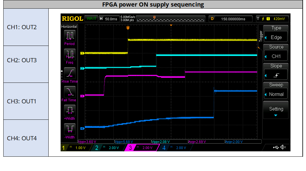
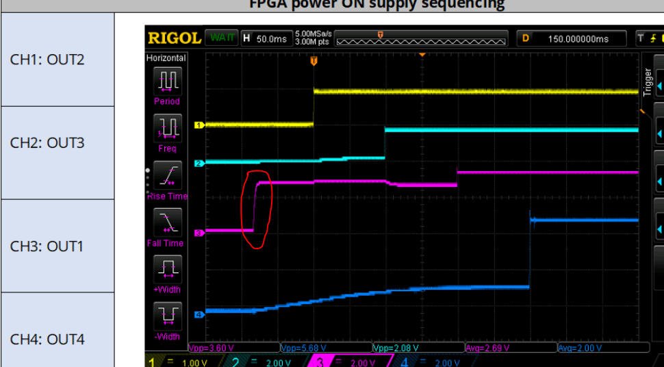
The goal is to turn ON power supplies in sequence OUT2 -> OUT3 -> OUT1 -> OUT4 with a microcontroller (over ENx pins). MCU sends a proper ENABLE sequence to TPS65400 (EN2->EN3->EN1->EN4) with 100ms delay in the between but OUT1 starts first (3ms after the power supply is applied to TPS65400) and gives 2.4V on the SW1 pin (without switching, pure DC signal). After the EN1 signal is pulled up, SW1 starts switching and OUT1 rises from 2.4V to 3V3.

On the figure below is visible that CH3 (OUT1) starts first (with wrong voltage, 2.4V instead 3V3).

NOTE: OUT1 has 2.4V ("DC" voltage, NO switching) even with global ENABLE (pin 23) pulled down.

We have that problem on all PCBs so it is not bad soldering or similar.

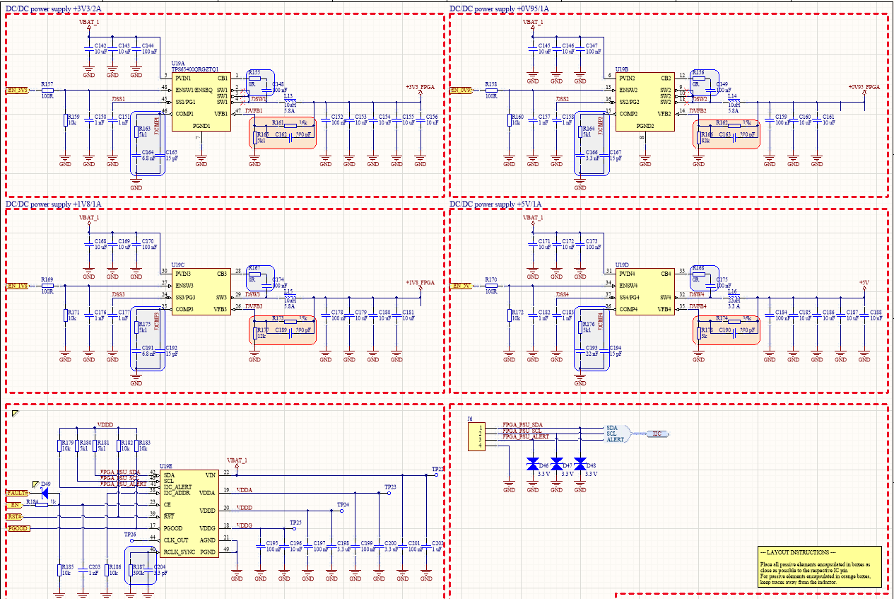
OUT1=3V3, OUT2=0V95, OUT3=1V8, OUT4=5V0

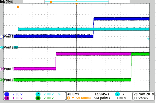
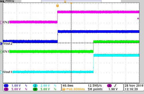
On the figure below is visible that OUT1 has 2.4V (NO switching) before EN1 (CH4) is applied. After EN1 is applied, SW1 starts switching and the output voltage rises from 2.4V to 3V3. OUT2 and OUT3 starts after EN2 and EN3 are received from MCU (oscilloscope is only 4 channel so EN2 and EN3 are not captured here).

  • Hi Kresimir,

    Can you upload your schematic? 

    Thanks,

    Lishuang

  • All ENx, FAULT, RST and PGOOD are connected to MCU.

    Al TPS65400 settings are a default (did not try programming over I2C).

  • Hi Kresimir,

    I checked the SCH, it looks okay.

    From the above waveform, I also found that CH2 OUT3 and CH4 OUT4 had little voltage before EN come.

    1. Is it possible to disconnect the output circuit (3V3_FPGA, 1V8_FPGA...)of the 4 channels?

    2. If it can be disconnected, could you change the power up sequence? For example, from  OUT2 -> OUT3 -> OUT1 -> OUT4  to OUT1-->OUT2 -->OUT3 -->Out4 or any other sequence.

    3. If it is okay, please upload the layout.

    Thanks,

    Lishuang

  • ....."From the above waveform, I also found that CH2 OUT3 and CH4 OUT4 had little voltage before EN come."

    Yes, 5V rises up to 1V before EN4 signal.

    ...."2. If it can be disconnected, could you change the power up sequence? For example, from  OUT2 -> OUT3 -> OUT1 -> OUT4  to OUT1-->OUT2 -->OUT3 -->Out4 or any other sequence."

    Yes, but only for testing purposes.

     Is it possible to "fix" this issue somehow with programming sequence over i2C?  Does TI have software (programming tool) for TPS65400? 

  • Hi Kresimir,

    Yes. I know it is only for testing purposes. I want to check the issue is from TPS65400 or from the output of 4 channels.

    And it is okay to using I2C to verify different sequence. We have the software on ti.com design&development page which is called PI-Commander-PMU EVM GUI. If you have EVM and cable at hand, you can have a try.

    We have tried various timing combinations and found no similar problems. You can try at your side and I will also check it.

    Thanks,

    Lishuang

  • Hi Kresimir,

    I have tested it using EVM and PMBus-I2C like below. All worked well.


    So please check that at the point of red circle in below picture, what is the system's action? Due to SW is not switching, so I think TPS65400 is not the root cause.

    Thanks,

    Lishuang

  • Hello,

    ..."Due to SW is not switching, so I think TPS65400 is not the root cause."

    Yes! You are right! The root cause in not in TPS65400, but in the MCU software. MCU pulls high lines connected to FPGA before FPGA is supplied. So, those lines act like a stray power supply.

    Now I need to prove this. But anyhow, the problem is elsewhere not in TPS65400.

    Many thx for your support.