This thread has been locked.

If you have a related question, please click the "Ask a related question" button in the top right corner. The newly created question will be automatically linked to this question.

DCR010505: DCR010505 failure_SYNC pin Low resistance

Part Number: DCR010505

Hi,

I have the same problem which discrabed in the web: https://e2e.ti.com/support/power-management/f/196/t/612580?tisearch=e2e-sitesearch&keymatch=DCR010505#pi320995filter=all&pi320995scroll=false 

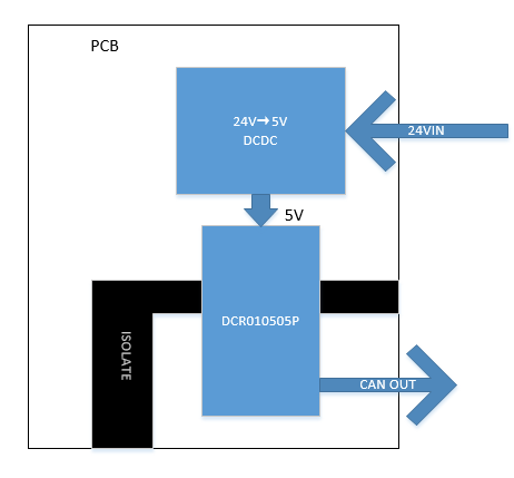
After I updated the software of  DSP on PCB and puted it back to cabinet,the 5V was not available.

The difference is that the SYNC PIN was floating on my board and the resistance was likely 20Ω to the -VS .

Could you please tell me what is the failure and cause of failure?

thanks.

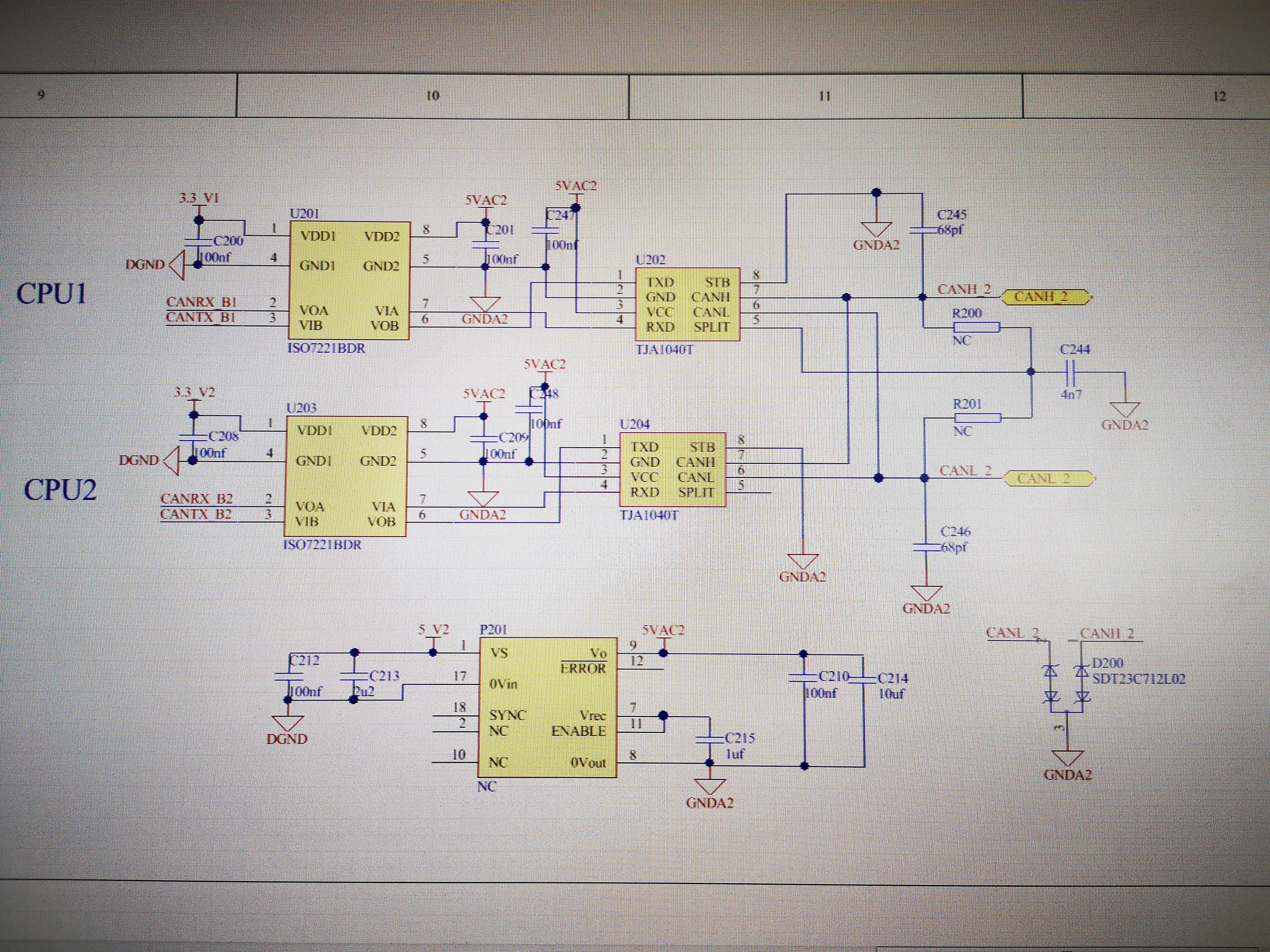
Refer to the schematic below:

  • Hi,

    I will loop in an application engineer who has more information on this. As it is around the holiday season, a response will be delayed. Please expect an answer by next week at the earliest. 

    Regards,

    Jimmy 

  • Hello,

    Unfortunately, the Applications Engineer who supported that previous post you mentioned is no longer with the team. Plus, the DCR010505 is part of our legacy devices which are +15 years old, so gathering information is a bit more challenging.

    Stated below are a few possible reasons for such failure: the device might of experienced an electrical over stress (EOS) after placing the PCB back on board.

    • Ensure the input voltage/current sources are capable of tolerating initial surge current
    • Ensure the design complies with all datasheet values
    • If the system is design for a hot-plugging application (ex. USB), ensure that the design tolerates side effect of hot plugging, such as, inrush current and voltage sag.

    Regards,
    Alejandro

  • Perhaps we can take a look at your schematic? (catch any potential shortage issues) We strongly believe an EOS occurred when placing back DSP on PCB.

    Thanks,
    Alejandro

  • Hi,

    Sorry I can't upload the schematic,but I take a picture as below.

    Maybe the failure was because of EOS,but how could I confirm it?

    On more thing,the batch number of all the  7 failure samples is 7CZEG2H,is it a coincidental or something ?

    Thanks

  • I reviewed your schematic and everything seems okay. Lets try this: Compare impedance on your non-functioning units to a normal operating unit.

    1. Check the impedance on all input pins. Probe continuity test:
      1. -VS (-probe) to Sync (+probe) = ?Ω
      2. +VS (-probe) to Sync (+probe) = ?Ω
      3. -VS (-probe) to +VS (+probe) = ?Ω
    2. Perform continuity test  with the probes reversed. Record results. [Example: -VS (+probe) to Sync (-probe) = ?Ω]
    3. Compare results of failed vs working units

    A hot plug-in can increase the peak pulse during intermittent connection stressing the primary controller. The block diagram below shows the input controller IC. So, by performing the test recommended above, the results can conclude that the primary controller has been over stressed (EOS).

    Thanks,
    Alejandro

  • Can we get an update on the measurements that Alejandro requested in his previous message?

    Regards,

    Jimmy

  • Hi,

    We have not heard back from you for some time. Can you provide us with an update on some of Alejandro's questions/requests?

    Regards,

    Jimmy 

  • Sorry for so late,here is the result and the block diagram of my board shows as below.

    non-functioning unit:

    1. -VS (-probe) to Sync (+probe) = 28.8Ω
    2. +VS (-probe) to Sync (+probe) = 7.1MΩ
    3. -VS (-probe) to +VS (+probe) = ∞Ω
    4. -VS (+probe) to Sync (-probe) = 28.8Ω
    5. +VS (+probe) to Sync (-probe) = ∞Ω
    6. -VS (+probe) to +VS (-probe) = 7.2MΩ

     normal operating unit:

    1. -VS (-probe) to Sync (+probe) = ∞Ω
    2. +VS (-probe) to Sync (+probe) = ∞Ω
    3. -VS (-probe) to +VS (+probe) = ∞Ω
    4. -VS (+probe) to Sync (-probe) = 15MΩ
    5. +VS (+probe) to Sync (-probe) = ∞Ω
    6. -VS (+probe) to +VS (-probe) = 6.4MΩ

    block diagram:

    Thanks

  • Sorry for so late,here is the result and the block diagram of my PCB:

    non-functioning unit:

    1. -VS (-probe) to Sync (+probe) = 28.8Ω
    2. +VS (-probe) to Sync (+probe) = 7.1MΩ
    3. -VS (-probe) to +VS (+probe) = ∞Ω
    4. -VS (+probe) to Sync (-probe) = 28.8Ω
    5. +VS (+probe) to Sync (-probe) = ∞Ω
    6. -VS (+probe) to +VS (-probe) = 7.3MΩ

    normal operating unit:

    1. -VS (-probe) to Sync (+probe) = ∞Ω
    2. +VS (-probe) to Sync (+probe) = ∞Ω
    3. -VS (-probe) to +VS (+probe) = ∞Ω
    4. -VS (+probe) to Sync (-probe) = 15MΩ
    5. +VS (+probe) to Sync (-probe) = ∞Ω
    6. -VS (+probe) to +VS (-probe) = 7.1MΩ

    Block diagram:


    Thanks.

  • Hello,

    Was there a pattern across your non-function units? The impedance on your non-function unit of SYNC to GND is lower than expected. Agains, safest conclusion would be that the parts experienced an EOS.

    Regards,
    Alejandro

  • Hi:

    There wasn't any pattern across the non-function units.What else should I do next?

    Thanks

  • Hi,

    I'd like to chime in here and ask how often these issues occur and if you can replace the failing unit with a new unit and test for reliability in your application. 

    From Alejandro's comments, he believes it is safe to assume the device may have been damaged somehow. The best way to test this is with a new unit to understand failure rate and operating conditions that might cause EOS.

    Can you please test this?

    Regards,

    Jimmy