This thread has been locked.

If you have a related question, please click the "Ask a related question" button in the top right corner. The newly created question will be automatically linked to this question.

TPS2553: About reverse-voltage protection

Part Number: TPS2553

Hello support team,

I have a question about the “reverse-voltage protection” function of TPS2553.

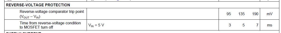
What is the voltage range of VIN where “reverse-voltage protection” works under the condition of VOUT – VIN> 135 mV?
Could you teach me in point of view whether or not reverse current flows from VOUT to VIN.
I don't care whether the FAULT output works or not.

Looking at "7.5 Electrical Characteristics" on page 7 of the datasheet, IREV : Reverse leakage current is 1 µA (MAX) under conditions of VIN = 0 V and VOUT = 6.5 V.
So I think “reverse-voltage protection” may work even if VIN is 0 V. Is my understanding correct?

Sincerely,
M. Tachibana

  • Hi Sir,

    1. Yes. Current flows from Vout to Vin.

    2. Yes, it works as VIN=0V.

    For TI's policy, I will first click resolved button.

    If you have any other concern, contact me any time.

    If you think resolved, please help click 'Issue is solved button'.

    Thanks.

  • Hi Zhang-san,

    Thank you for the reply.
    But I did not understand well.

    You answered that reverse current flows in No.1, does that mean that the “reverse-voltage protection” does not work?

    Or is that mean that the reverse is current as small as the leakage current and the “reverse-voltage protection” works when VIN is from 0 V to VOUT - 135mV?

    Sorry to trouble you, but please teach me again.

    Sincerely,
    M. Tachibana

  • Hi,

    It's just two situation:

    1. Vin above zero. The IC works. With Vout-Vin>135mV, after 5ms, will turn off MosFet. During the 5ms, current will flow from Vout to Vin. 

    2. Vin=0V, internal FET will not be open, the current from out to input will be blocking. Only with 1uA leakage current.

    For TI's policy, I will first click resolved button.

    If you have any other concern, contact me any time.

    If you think resolved, please help click 'Issue is solved button'.

    Thanks.

  • Hi Zhang-san,

    Thank you for your reply.
    I’d like to get a better understanding just in case.

    My understanding is as below;
      Where VIN is from 0V to VOUT-135mV,
        the reverse current flows from VOUT to VIN for 5ms,
        and internal MOS-FET turns off after 5ms and only the leakage current flows.
    Is it correct?
    What I want to know is the behavior after 5ms.

    I'm sorry to ask you many times, but please teach me again.

    Sincerely,
    M. Tachibana

  • Hi,

    1. hat's right. As Vout bigger than VIN 135V, current will flow from Out to IN for 5ms. And then turn off internal MOS, only leakage current.

    2. VIN=0V, meaning the internal MOSFET is disabled. So no matter how much the voltage is of Output, OUT current will not flow to input. Only leakage current.

    For TI's policy, I will first click resolved button.

    If you have any other concern, contact me any time.

    If you think resolved, please help click 'Issue is solved button'.

    Thanks.

  • Hi Zhang-san,

    I understood.
    Thank you for your kindness despite my repeated questions.

    Respectfully yours,
    M. Tachibana