Hi
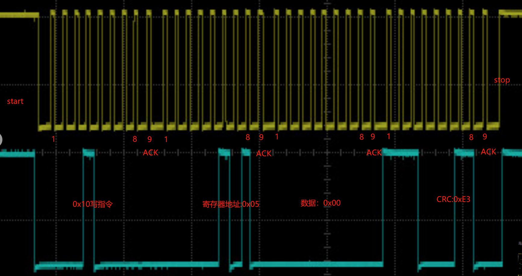
GeneralReturnType BqIf_SetDeviceByte(uByte addr,uByte data)
{
uByte i = 0;
uByte wr_crc;
uByte calc_crc_data[3];
__DI();// Off interrupt
calc_crc_data[0] = BQ76940_WR;
calc_crc_data[1] = addr;
calc_crc_data[2] = data;
wr_crc = crc8_check(calc_crc_data, 3)// calculate CRC
// write 3 times until write ok
for(i = 0; i < 3; i++)
{
BqIf_IICStart();//
BqIf_WriteByte(BQ76940_WR);
if(BQIF_ERR_OK != BqIf_IICAckDevice())
{
BqIf_IICStop();
continue;
}
BqIf_WriteByte(addr);
if(BQIF_ERR_OK != BqIf_IICAckDevice())
{
BqIf_IICStop();
continue;
}
BqIf_WriteByte(data);
if(BQIF_ERR_OK != BqIf_IICAckDevice())
{
BqIf_IICStop();
continue;
}
BqIf_WriteByte(wr_crc);
if(BQIF_ERR_OK != BqIf_IICAckDevice())
{
BqIf_IICStop();
continue;
}
BqIf_IICStop();
break;
}
__EI();
if(i >= 3)
{
return BQIF_ERR_WR;
}
return BQIF_ERR_OK;
}
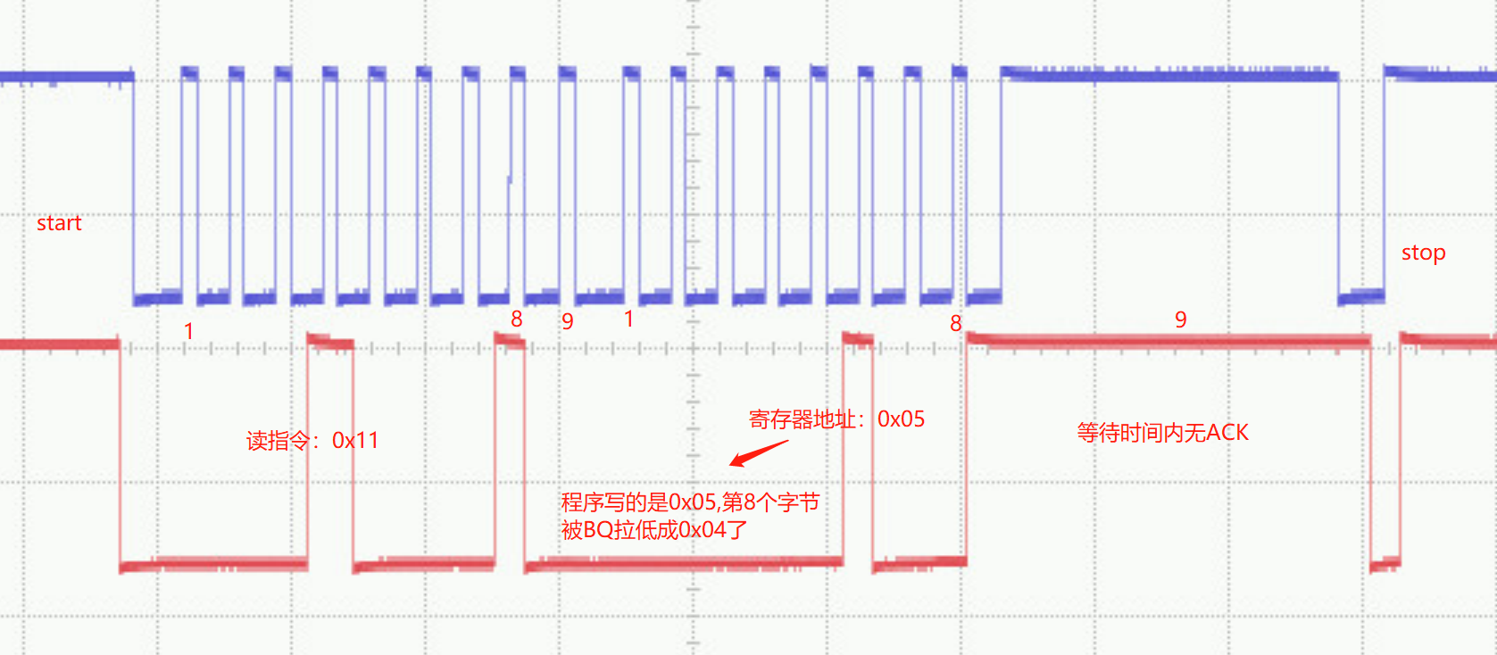
__DI();
BqIf_IICStart();
BqIf_WriteByte(0x11);
if(BQIF_ERR_OK != BqIf_IICAckDevice())
{
}
BqIf_WriteByte(0x05);
if(BQIF_ERR_OK != BqIf_IICAckDevice())
{
BqIf_IICStop();
}
else
{
BqIf_IICStop();
}
__EI();