Hi Team,
I didn't understand what you want to tell us in following two sentences in datasheet, 10.1 Layout Guidelines. Can you supplement the details?
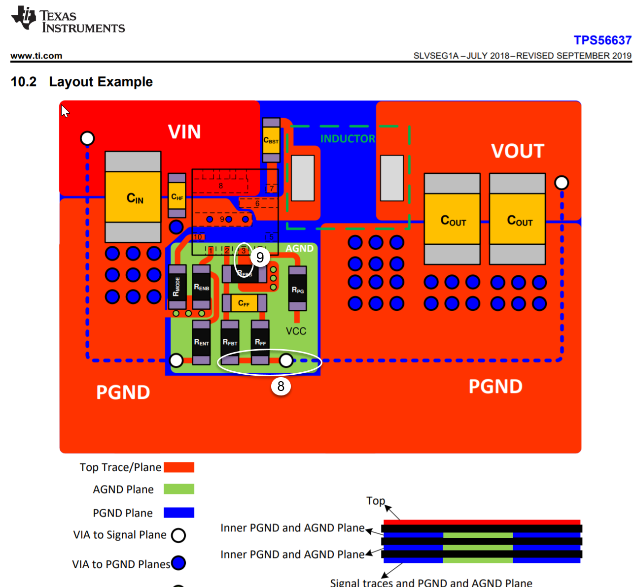
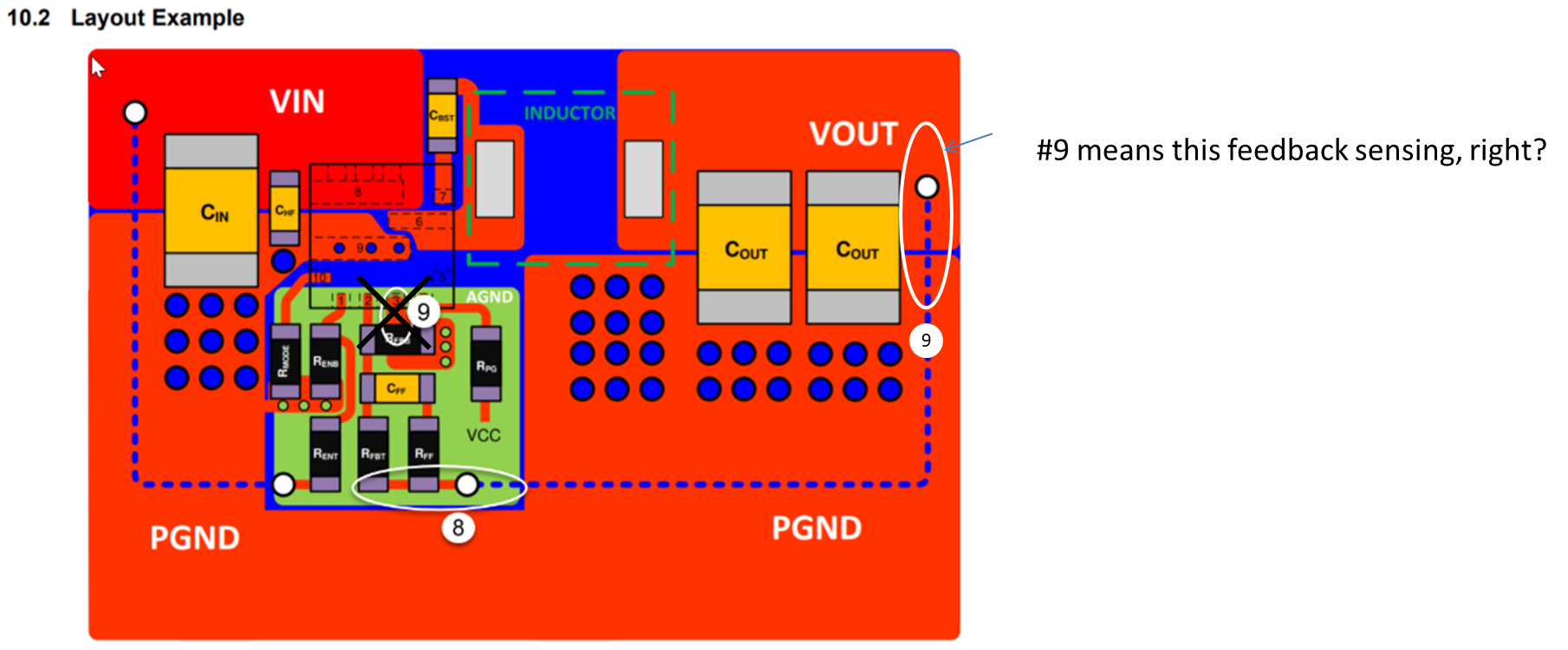
8. A separate VOUT path should be connected to the upper feedback resistor.
9. Make a Kelvin connection to the GND pin for the feedback path
Regards,
Takashi Onawa