This thread has been locked.

If you have a related question, please click the "Ask a related question" button in the top right corner. The newly created question will be automatically linked to this question.

LMG1205: HO and LO resonance effects

Part Number: LMG1205
Other Parts Discussed in Thread: LMG1210

We are using the LMG1205 as a driver for a GaN Halfbridge made of EPC2001C FETs.

Lately we had some issues with FETs burning under certain conditions (switching high currents).

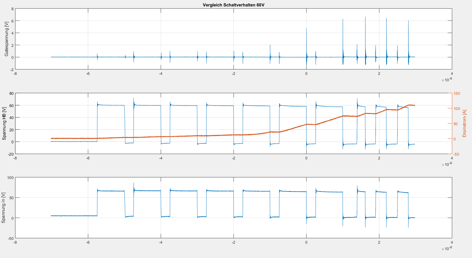
To find out the cause of this behaviour we performed a double-pulse test. We saw an oscillation on the gate signals dependent on the current we switched.

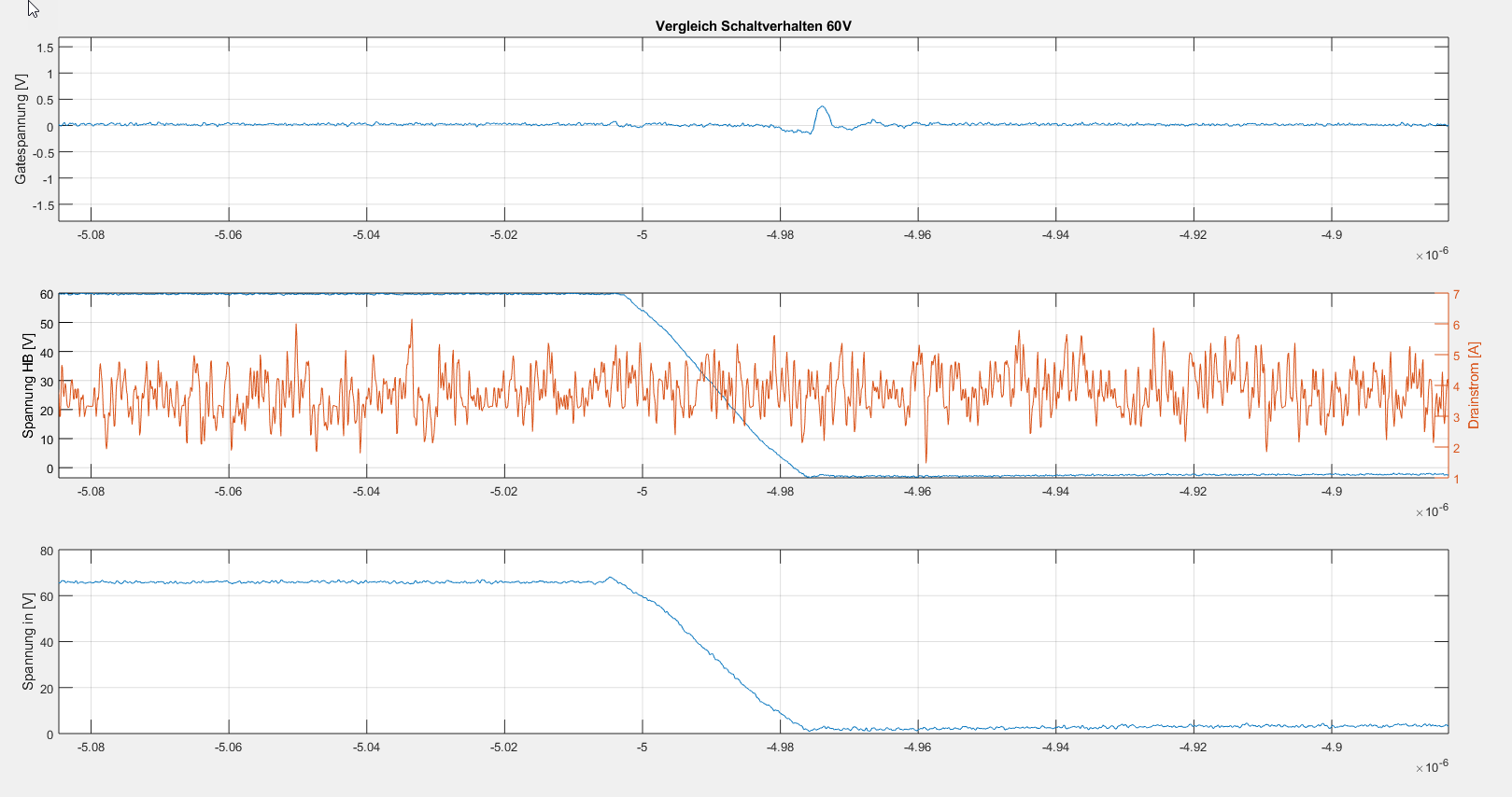
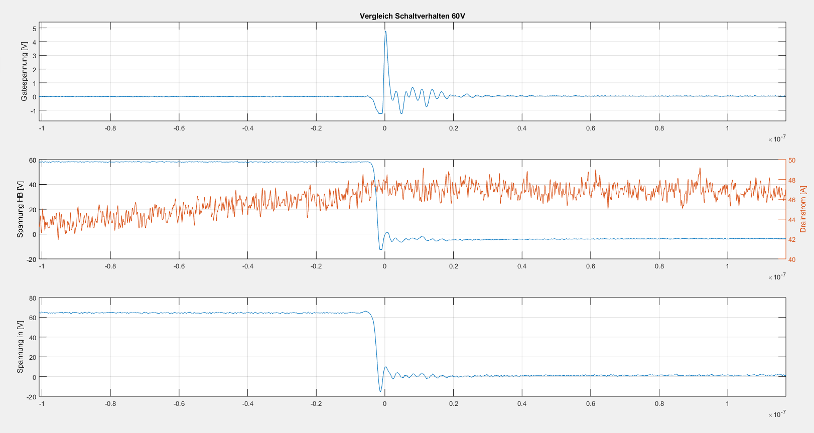
In our view the problem is caused by a high dU/dt (gets even higher the higher the current is) which causes a current across miller capacity and causes an impact on the gate voltage. 

But we are a bit concerned about the overshoot which follows afterwards (causes cross-conduction). It is an oscillation with about 300MHz.

But now to my question:

I know, the exact behaviour is an interaction of FET, driver and PCB. But our guess is that the oscillation is caused by a resonance of the driver output (maybe the bodydiode of the output stage?).

Do you have any data about the transition behavoiour of the outputs? Are there any resonance frequencies?

  • Hi Thomas,

    Thanks for reaching out about lmg1205. Which fet is burning? Is 1205 burning as well?

    Can you explain in more detail the double pulse test?

    Are you using the first pulse to set the inductor current and the second pulse to see the effects of the gate during turn off?

    If there is 300Mhz ringing on the gate, it's possible this is PCB layout related or measurement probe related. During normal operation, Can you take a waveform of the lmg1205 output with pig tail probe points? This waveform should be the same as the epc gate waveform. Can you also waveform the switch node to see if the power loop is ringy as well?

    Can you send the sch and layout portion of 1205 for review? Tightening up the gate and power loop can reduce PCB inductance and ringing during high dv/dt.

    Thanks,

  • Hi Jeff,

    thanks for your reply!

    Due to crossconducting both FETs fail. We observed defect LMG1205 as well what may be caused by a short circuit to the gatepin when the FETs fail (due to vaporised solder or internal short).

    Double Puls Test:

    We put the inductor parallel to the lowside switch and then switched the highside by giving a certain number of pulses (out of a frequency generator) to the HI pin of LMG1205.

    The same we did for the lowside switch (inductor parallel to highside).

    With this procedure the current rises with every puls and switching behaviour at different currents can be observed.

    We already used pigtail probes for measuring the voltages. as our gate loop is very small and we do not use an external gate resistor the output of the LMG1205 and the measured gate voltage should be the same.

    We processed our oscilloscope data in matlab to be able to have a closer look. We used 2.5GHz oscilloscope so bandwith is limited to 500MHz of the probes what should be sufficient for this measurement.

    I attached three figures with three plot each:

    --> first plot: gatevoltage of the lowside (LO-voltage)

    --> second plot: switching node and output current

    --> third plot: gatevoltage of the highside (HO-voltage)

    Figure 1: overall plot of the doublepulse test (sitching the highside with inductor parallel to the lowside)

    Figure 2: zoom at t=-5µs, where the ringing is very small (swtiching about 4A)

    Figure 3: zoom at t=0µs where the ringing is high and leads to parasitic turnon (switching about 45A)

    Best regards

    Thomas

  • Hi Thomas,

    Thanks for the update,

    Can you tell me the maximum dv/dt  for figure 3?

    What dead-time is being used? does the issue happen with 10-20ns longer dead-time?

    is this for motor drive application?

    Have you considered using LMG1210 which has 300V/ns CMTI rating as well as PWM mode to control a precise dead-time?

    Thanks,

  • Hello Jeff,

    maximum dv/dt of figure 3 is about 50kV/µs and the dead time is about 30ns -> normally we do have light load conditions so the dead time was chosen quite high.

    The circuitry is within a motor drive application but the LMG1205 and GaN Fets are used in a kind of DCDC-Converter.

    We have not considered LMG1210 yet. I think other measures can be taked if we know exactly why the failure occurs.

    Due to that I asked the question about resonance effects. Do you have measurements/data of the behaviour of LMG1205?

    Best regards

    Thomas

  • Hi Thomas,

    Thanks for the update, lmg1205 has a cmti rating of 50V/ns max. That means if the part sees a slew rate on HS this high it can corrupt the input signal or negatively impact the driver output. To lower the dv/dt on HS try using a 2-10ohm gate resistor to slow the switching transition down and test under the same conditions. If the max cmti can stay under 50v/ns its possible this issue can be fixed.

    Thanks,

  • Hi Jeff,

    in the meantime we found out that the 300MHz ringing might come from the FET itsself because we even see it in a simulation with the manufacturers model.

    But your hint explains why the circuitry behaves odd at even higher currents (even faster slopes). 

    Thank you very much for your support!

    Thomas