This thread has been locked.

If you have a related question, please click the "Ask a related question" button in the top right corner. The newly created question will be automatically linked to this question.

UA78M: Vout Problem

Part Number: UA78M
Other Parts Discussed in Thread: TPS7A83A, TPS7A90, UA78

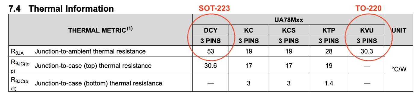
Device: uA78M05IDCYR
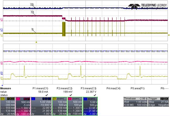
Vin: 22V

Vout: 5V

Iout:50mA

Problem Description: When Input voltage is up to 22V with 50mA(ambient Temp is 25degree), the output voltage becomes abnormal and eventually dropping down to 0V. Why?

In the d/s, it says the there is coming with Internal Thermal-Overload protection. What's the triggered conditions? What's the max. power rating on chip?

Please see the tested waveform here. 

Please help on this problem. thanks. 

  • Hi Brian,

    At 22VIN and 5VOUT at 50mA, this is dissipating 0.85W. Based on the thermals for the packages, this should not at all be an issue:

    The worst-case in a KTT package, this is only a 21.5C rise above ambient. Now that being said, the TJA numbers are assuming a JEDEC standard High-K board. 

    Are you testing with the device mounted on a PCB? 

    The datasheet is not clear on where the thermal protection kicks in, but since the absolute maximum junction temperature is listed at 150C, I would suspect in kicks in somewhere around this temperature. 

    Here is a really good article on thermals.

    I hope this helps.

  • "At 22VIN and 5VOUT at 50mA, this is dissipating 0.85W"--> How to calculate the loss?

    The device is mounted on the PCB. I use another uA78M05IDCYR IC at 20VIN and 5VOUT at 150mA, and the output still abnormal 

    Is there any limitation of the IC using?

  • Hi Brian,

    The power loss across a linear regulator is (VIN-VOUT)*IOUT+VIN*IQ(LOAD)= W. Normally we only focus on (VIN-VOUT)*IOUT as the 2nd term is often negligible when compared to the first.

    In your example:

    VIN=22V

    VOUT=5V

    IOUT=50mA

    So the power dissipated across the regulator is (22-5)*0.15A=2.55W

    The 2nd term would be 22V*0.006A or 0.132W so the total power dissipation is actually closer to 2.68W

    So if you are using the SOT-223 package, the TJA is 53C/W

    53C/W*2.68W=142C temperature rise above ambient. Now, this is the ambient of your PCB, not necessarily the ambient of the room. So if the PCB is around 40C, this means the die temperature could rise to around 182C

    The datasheet is not clear on where the thermal shutdown kicks in, but the recommendation is to keep the junction below 125C. I may be safe to assume thermal shutdown kicks in around 160C. 

    I hope this answers your question.

  • The power loss across a linear regulator should be VIN*Iin-VOUT*IOUT,  the value will smaller than you give.  and the Ta is about 25degree and the other function of the product is not work, so the PCB temperaure must lower than 40C.

    How to define the ambient point?

    the test condition is not over the spec, but why the output voltage is abnormal?

    Is there any limitation for this IC? 

    Besides, i have anorher test for under condition, but the output also abnormal.

    CH2:Vin: 20V

    CH4:Vout:5V

    CH1:Iout: 100mA


  • HI Biran,

    The primary power dissipated in any linear regulator is (VIN-VOUT)*IOUT. If you consider the IQ of the device, then you add VIN*IQ to this expression.

    For the above example, if VIN is 20V, and VOUT is 5V at 100mA, just considering the first term of the expression we have:

    (20-5)*0.1 or 1.5W. The TJA for the SOT-223 package is 53C/W so 1.5*53=79.5C rise above the ambient. Adding in the 2nd term VIN*IQ, this is 20V*0.006A or 0.12W. Therefore the total temperature rise should be 1.62W*53C/W or 85.9C above ambient. Note: the 53C/W is on a Jedec standard High-K board, but that is not at all an ideal layout. Here is an application report showing how layout impacts thermal performance.

    The Ambient is defined as the ambient temperature of the device in your application. Meaning, the temperature of the PCB when then the device is running.

    To answer your question on the limitation for the IC, for long-term reliability it is recommended that you design to ensure that the operating junction temperature is less than 125C. The device's internal protection will protect itself with its own thermal and over-current protection.

    I hope this clarifies your question.

  • What does "Jedec standard High-K board" mean?

    Could you provide the layout for the value in datasheet?

    Which part number should i take as reference in  application report    for uA78M05IDCYR(SOT-223) ,Because there is no same part number and package type

  • Hi Brian,

    The JEDEC standard is a free download. The link is here: https://www.jedec.org/sites/default/files/docs/jesd51-12.pdf

    You just have to register. 

    This is a standard layout that is used to easily compare thermal parameters between similar packages. It is NOT an ideal layout. Our datasheets use thermal parameters assuming a JEDEC standard High-K board. 

    The application report illustrates how different layouts can impact thermal performance and the key take-away is the better the copper pour around the thermal pad, the better the performance. 

    You can confirm that the device is going into thermal shutdown by simply lowering the input voltage with the same load current. If you have space, moving to the TO-252 package would help a lot. 

    WIth the TO-220 package, with VIN at 20V and VOUT at 5V at 100mA, the device still dissipates 1.5W (1.62W considering IQ). So the thermal rise above ambient would be ~49C vs. ~86C. Again both numbers would be a bit lower with a proper layout. 

    I hope this helps.

  • In  application report , what is signal in the layer 1 and layer 2?

    Could you provide the layout file(.PCB ,etc) for TI testing to compare different between our design and datasheet measurement (trace width, via number ,etc)

    What is the max power loss for UA78M05IDCYR(SOT223) and other package?

    What is the max input voltage for UA78M05IDCYR?

    What is the max output current at max input voltage and Ta=25C for UA78M05IDCYR

    Is there any design guideline for LDO we can refer?

  • Another Question

    If datasheets use thermal parameters assuming a JEDEC standard High-K board, how can the real TJA and steady junction temperature in our PCB be known? 

    Can you check the precise shunt down temperature for uA78M05IDCYR, so that we can design for max output current

    Thank!

  • Hello JC,

    Happy New Year!

    Customer would like to estimate the PCB cooling area for the uA78M05 SOT-223 package. Could you offer the thermal resistance Information or simulation results of uA78M05? With this, customer can try to estimate the pcb area on the critical design. (The board has been in the mass-production, customer don't prefer to modify the PCB greatly)

    For example: Relationship between the copper area and the thermal resistance θJA and power dissipation.

    below diagrams are obtained from other supplier. 

  • Hi Yuwei,

    Sorry for the long delay. I was out of office for the holidays in the US.

    2s2p in the JEDEC refers to a board with 2 signal planes (ideally for signal routing) and 2 power planes. The signal planes do not contribute much at all to the thermal performance of the board. This makes more sense when looking at more complex LDO's like the TPS7A90 or TPS7A83A. 

    To answer your other questions:

    What is the max power loss for UA78M05IDCYR(SOT223) and other package? *The UA78 has thermal protection so it will self protect if thermally the die becomes too hot. For reliable design, you want to make sure your design is such that Tj is less than 125C. So the TJA parameter for the desired package will help to estimate this. 

    What is the max input voltage for UA78M05IDCYR? *The absolute maximum input voltage is 35V. Recommended maximum is 30V

    What is the max output current at max input voltage and Ta=25C for UA78M05IDCYR *See below for this and the question above:


    Is there any design guideline for LDO we can refer? *The application report recommended above is really the best for understanding how the layout can optimize thermal performance. 


    I hope this helps to answer your question. 


  • Hi Brian,

    We do not have this for the UA78 but we are bringing a thermal widget online that will do the same. Let me see if I can prioritize the UA78.

    Regards,

  • Do TI have imformation about thermal resistance vs copper area for SOT223 package?

    Can we try to use the thermal widget online by ourself?

    Thank!

  • Hi Brian,

    the TJA parameter is the best for predicting the potential thermal rise in the application.

    If you want to use a thermal widget to compare with another SOT-223 package, that will give you an idea but the two key parameters for determining thermal performance are the package and the area of the die. I am pushing the packaging team to get the UA78 thermal widget done ASAP so you can get more precise estimates. 

    I hope to get some feedback today.

    Regards,

  • Hi Brian

    Is there any update about result?

    Thank!

  • Hello John,

    Could you possibly reply if you get info from design team? Very thanks. 

    Regards

    Brian

  • Hi Brian,

    The thermal data comes from the packaging team. I have been pushing to add the UA78 to the thermal widget. An example of which can be found here: 

    https://www.ti.com/product/TLV1117?utm_source=google&utm_medium=cpc&utm_campaign=app-null-null-GPN_EN-cpc-pf-google-wwe&utm_content=TLV1117&ds_k=TLV1117&DCM=yes&gclid=Cj0KCQiAjfvwBRCkARIsAIqSWlN9MG7w01hcE1a2XkedQa1iXIQF78YCN6P9Ow_tZZcL-Rc1UancZXwaAqsiEALw_wcB&gclsrc=aw.ds

    The above link is for the TLV117 ion the SON package but can give you an idea as to how copper weight and area can help with thermal performance. If I can get the UA78 added to this tool it would be much more accurate.

    Regards,

  • Hi Brian,

    I have been pushing to get this done. We ran into a hurdle in that the thermal widget was not designed for constant drop-out devices (i.e. drop-out does not change much as a function of load current). So this may take some more time to bring online. Meaning if we implement as is, the user could enter in VIN=9V and VOUT=8.0V and the tool would give a plot similar to what you show above. This is not possible.

    For the short term, the explanation above to use TJA to predict thermal rise is the best approach and then increasing the copper area only helps to improve that metric. 

    Once we optimize the thermal widget, I have a plan in place to add all of our popular devices.

    I will keep you posted.

  • Hi

    Is any updated?

    Thank!

  • HI Yuwei,

    We just had a discussion on this yesterday and the team is trying to confirm a date when we can update this.

    Hopefully soon.