This thread has been locked.

If you have a related question, please click the "Ask a related question" button in the top right corner. The newly created question will be automatically linked to this question.

LM5069: Delayed response to detect OVLO

Part Number: LM5069

Hello Team,

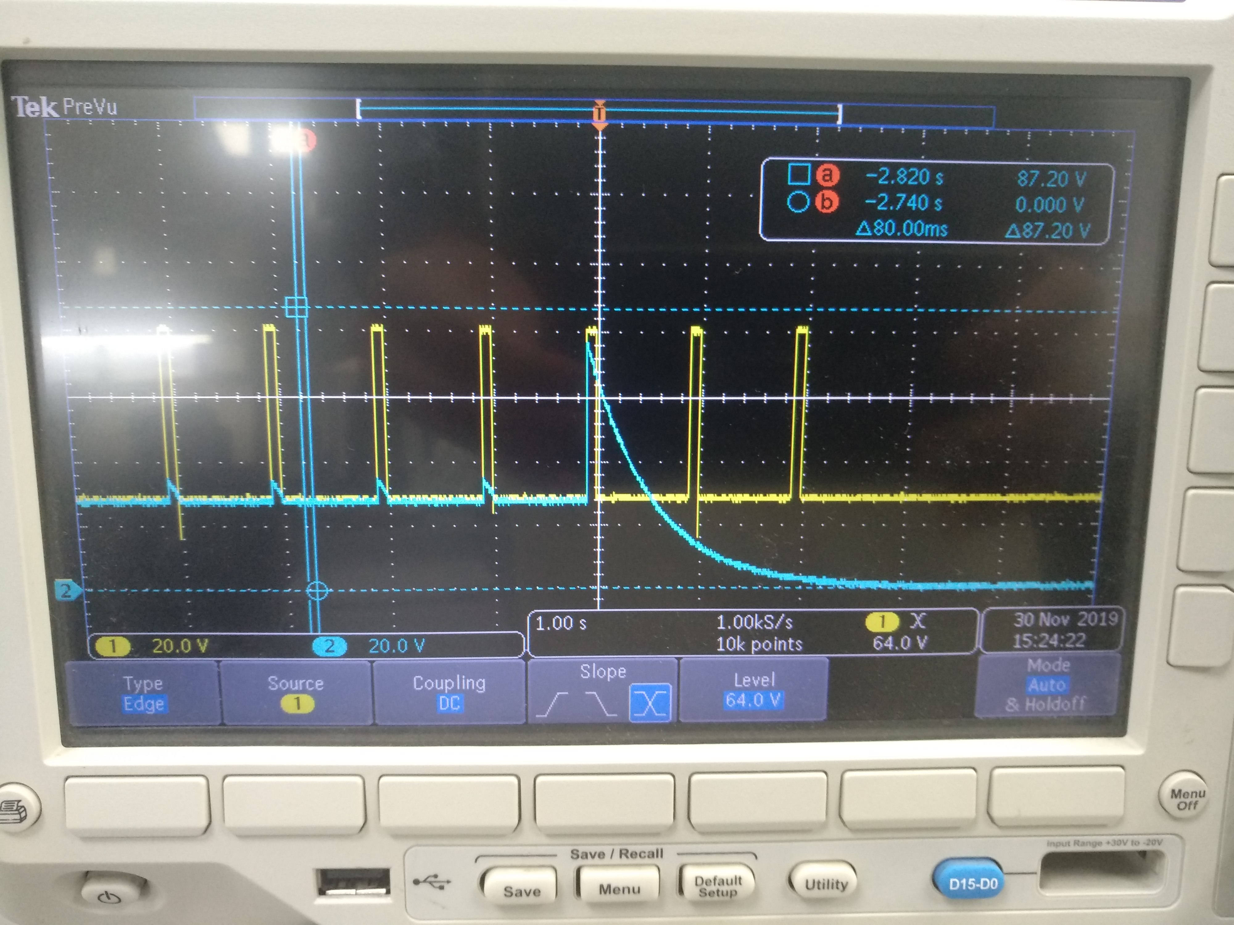
Currently my customers are using LM5069 in one of the circuit for OVLO (33V), UVLO(20V) and surge protection purposes (80V for 100ms), but this device needs greater than 55us to respond (the GATE pin to be LOW). Because of this 80V is coming at the output of LM5069 within 55us. Typical input operating condition of the device is 28V. Why this device is taking 55us to respond evenif OVLO detects, but in datasheet its mentioned 11us for the GATE to be LOW ?

  • Hi Mayank,

    Thanks for reaching out!

    11us is the delay response and is NOT the time to discharge the GATE to LOW. For OVLO event, the controller pulls down the GATE with 2mA pull-down current so, the discharge time depends on the effective capacitance at the GATE pin.

    Please try zener clamp at the GATE as shown in http://www.ti.com/lit/an/snva683/snva683.pdf and test.

    BR, Rakesh

  • Hello Sir,

    Thanks for your quick response.

    My customers implemented the said changes and have observed following results:

    They placed zener diode (36V clamping) with 500mW capability at the gate pin of LM5069. Following are the test case and its result.


    Test Case: 1

           Nominal input voltage of 28V DC and voltage spike pulse of 60VDC for a period of one second.

    Result: 1

           No failures observed (with and without 400mA load).


    Test Case: 2

           Nominal input voltage of 28V DC and voltage spike pulse of 70VDC for a period of one second.

    Result: 2

           failures observed (with and without 400mA load). Zener, pass elements (MOSFETS) got damaged and LM5069 body near pin 1 and 2 had visible burn mark.


    Test Case: 3

           Nominal input voltage of 28V DC and voltage spike pulse of 75VDC for a period of one second. With 62K series resistor to LM5069 gate pin.

    Result: 3

           failures observed (without 400mA load). Reverse voltage blocking diode (Maximum current of 250mA) get damaged.

  • Hi Mayank,

    Can you share the component details ... MOSFET part number, zener diode part number, Cout value.

    Also, provide some test waveforms for case-3. Please capture Vin, Vout, GATE and input current 

    Best Regards, Rakesh

  • Hello Sir,


    Please find below required details:


    Mosfet PN:- BSC035N10NS5ATMA1 (Infineon) Zener diode:- 36V, TZM5258B-GS08 (Vishay) Cout value = 20uF.

    Attached image is having input and output of LM5069 at burn out condition for case 3.


  • Hi Mayank,

    Can you please include GATE and input current as well.

    Also, add math function for (Vin-Vout)*input current to check the power stress on the MOSFET.

    Best Regards, Rakesh

  • Hi Mayank,

    Did you able to check the power stress on the MOSFET. ?

    Best Regards, Rakesh

  • Hi Mayank,

    I am closing it for the time being, please feel free to post updates to open it again.

    Best Regards, Rakesh