This thread has been locked.

If you have a related question, please click the "Ask a related question" button in the top right corner. The newly created question will be automatically linked to this question.

TPS54678: abnormal waveform on SW at low current

Part Number: TPS54678
Other Parts Discussed in Thread: TPS62866

Hi Team,

Here is one question from customer.

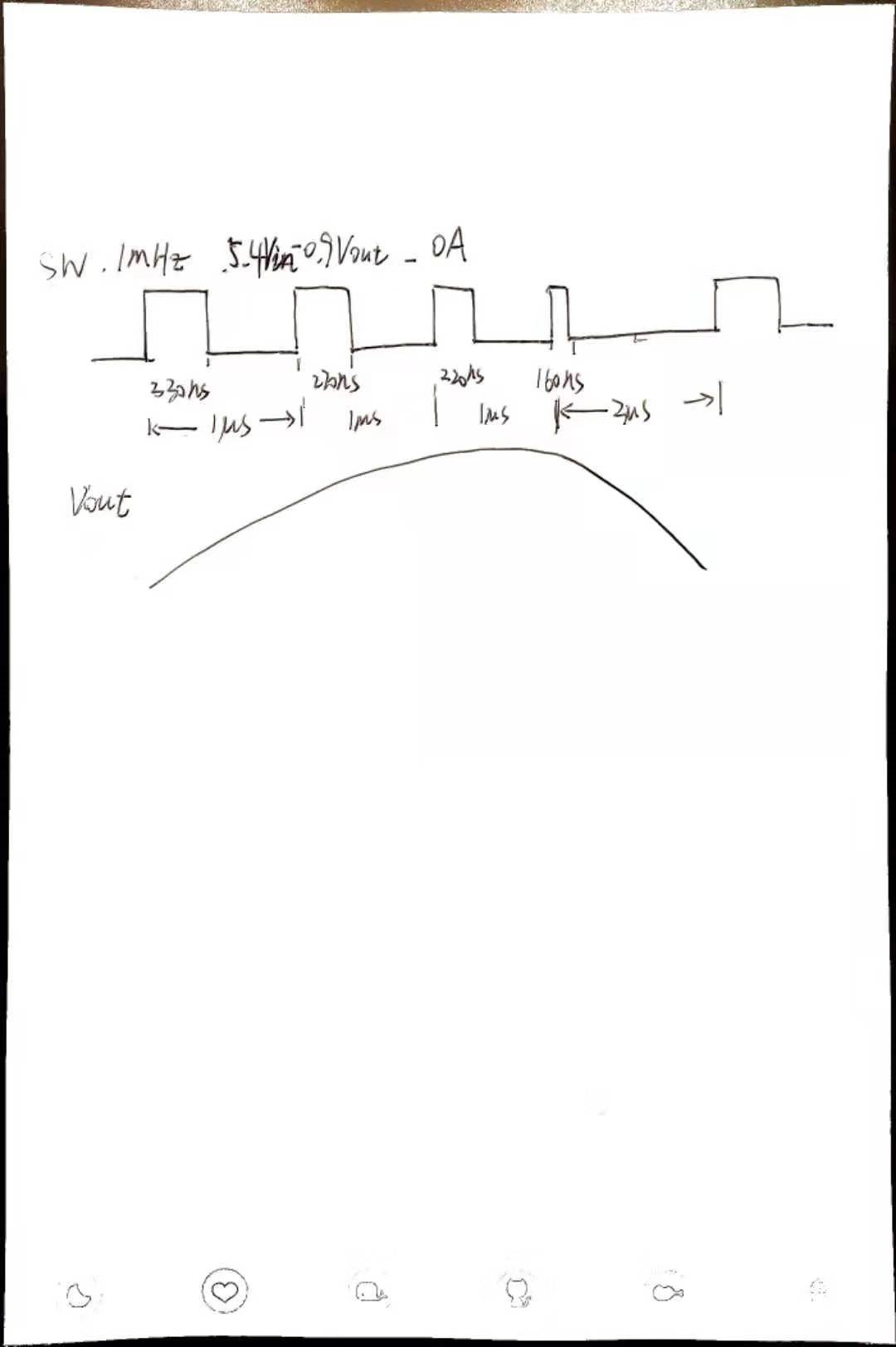
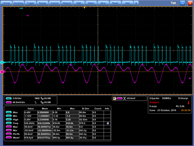
5.4Vin to 0.9Vout, Iout=0A, Fsw=1MHz,  you can see below SW waveform that Duty cycle changes.

a. increasing load to 1A, Duty cycle becomes stable.

b. change Vout to below 0.9V, the issue always there. Change Vout to high value, for example, 1.2V, no issue.

c. add 15pf cap on comp pin to gnd, Duty becomes stable.

d. decrease Vin below 5.4V, Duty becomes stable.

So it seems the issue is related with Duty.  I suspect it's related with noise on comp originally, but it cannot explain why there is issue with higher Vout and lower Vin.  From the waveform, it seems related with Ton-min, but not sure how to explain the waveform. 

Please kindly add your comments. Thanks.

BRs

Given

  • Hi Given,

    I am not quite sure to understand here, what you problem is.

    You are saying:

    "5.4Vin to 0.9Vout, Iout=0A, Fsw=1MHz,  you can see below SW waveform that Duty cycle changes."

    What you are describing is expected behavior at light loads for this part.

    At light load/ no load, duty cycle changes depending on the voltage the system sees at Vsns. Regulation of output depends on Vref accuracy as well.

    Furthermore, ton_min is 100ns typical and specified at 120 ns at no load.

    If the Vout variation at light load because of this constraint is not fitting your load specification.

    I would recommend the use of the TPS62866 which adapts its frequency at lower loads for efficiency improvement.

    Thank you very much!

    Best Regards,

    Dorian 

  • Hi Dorian,

    Thanks for your reply.

    what I mean is the Duty cycle should be stable when output is regulated even at light load. For example, for tps54678, in customer's application, if 5.4Vin to 1.2Vout, then SW is stable, duty cycle is also stable, Vout ripple should be small.

    But as described as above, when Vin is 5.4V, Vout regulation point is set to below 0.9V, then you can find SW is not stable, duty changes which makes Vout changes much.

    Thanks.

    BRs

    Given

  • Hi Dorian,

    To be clear,  my question is why duty cycles changes at such condition?  Is it due to Ton-min or due to loop stability or something else? Thanks.

    BRs

    Given

  • Hi Given,

    I would say that it is potentially due to the fact that the voltage gap between Vin and Vout is large.

    So here your limitation would be minimum Ton.

    I recommend you to have a look at the TPS62866 which does not have this limitation because at light load switching frequency will be reduced.

    Is fixed frequency a must have in your application?

    Thank you!

    Best Regards,

    Dorian   

  • Hi Dorian,

    customer's main question is on the reason why duty cycle changes currently. It will affect the Vout ripple.

    As you mentioned, it may be due to the voltage gap, could you please describe more details on how it affect the duty?

    On my side, 5.4V to 0.9V, 1MHz, Ton is 167ns,  and Tonmin is 120ns (max) , then it should still can be stable since there is margin . Also as mentioned, adding a 15pf Cff on comp, the SW becomes stable. So my initial suspect is the noise coupling on comp but when Vin is low or Vout is high,  there is no such issue. So it seems not just noise and has relationship with duty.

      Please kindly add your comments. Thanks.

    BRs

    Given

  • Hi Dorian,

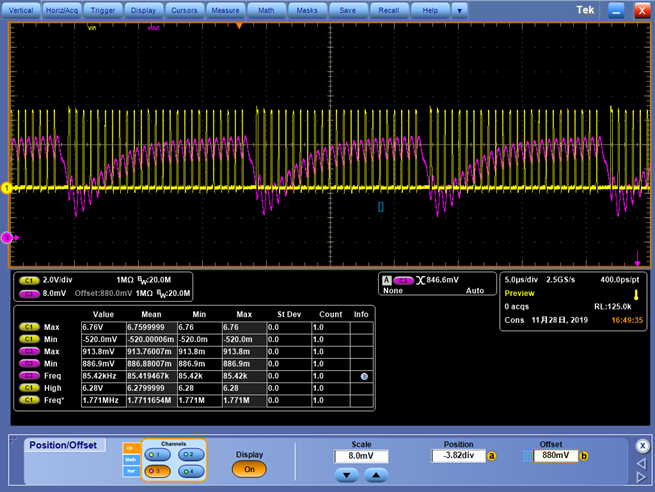
    In addition, please kindly see below waveforms.

    Vin=5.4V, Vout=0.9V, Iout=0A. Fsw=1MHz

    Increase Fsw to 1.77MHz, Vin=6.3V, Vout=0.9V, Iout=0A. This should has Ton-min limit. waveform as below

    Thanks.

    BRs

    Given

  • Hello Given,

    You mentioned: " adding a 15pf Cff on comp, the SW becomes stable. So my initial suspect is the noise coupling on comp but when Vin is low or Vout is high,  there is no such issue. So it seems not just noise and has relationship with duty."

    I think you are heading the right direction here. At no load, coupling noise can disturb the regulation of the system as well as if the layout of your system is not optimized. 

    Could you share the schematic and the layout of the system?

    Thank you very much!

    Best Regards,

    Dorian

  • Hi Dorian,

    Thanks for your reply. Will feedback to you once got the sch/layout from customer.

    But one more question, since it also happens at low duty cycle ( not just noise, since less gap between Vin and Vout doesn't has such issue) , could you please kindly help explain on this ? In my opinion, it doesn't make sense since normal Ton should be ~160ns at such condition which is above Ton-min(max) ( ~120ns). Thanks.

    BRs

    Given

  • Hi Given,

    As you said Ton is ~160ns, but theoretically Ton should be 120ns. 

    To my opinion, it is specifically because it is at low duty cycle (Vin>>Vout and no output load) that noise is affecting the regulation and customer is seeing those irregularities.

    Thank you!

    Best Regards,

    Dorian

  • Hello Given,

    I haven't heard back from you.

    Any update on your side? Do you have any further questions?
    Thank you very much!

    Best Regards,

    Dorian

  • Hi Dorian,

    Sorry for late reply.

    It takes time for customer to send out sch/PCB. I have discussed with them based on your reply and they'll check themselves.

    Will updated later if any more questions. I'll close the thread.

    Thanks for your support.

    BRs

    Given