This thread has been locked.

If you have a related question, please click the "Ask a related question" button in the top right corner. The newly created question will be automatically linked to this question.

LMG3410R070: Device failed during operation

Part Number: LMG3410R070
Other Parts Discussed in Thread: ISO7831

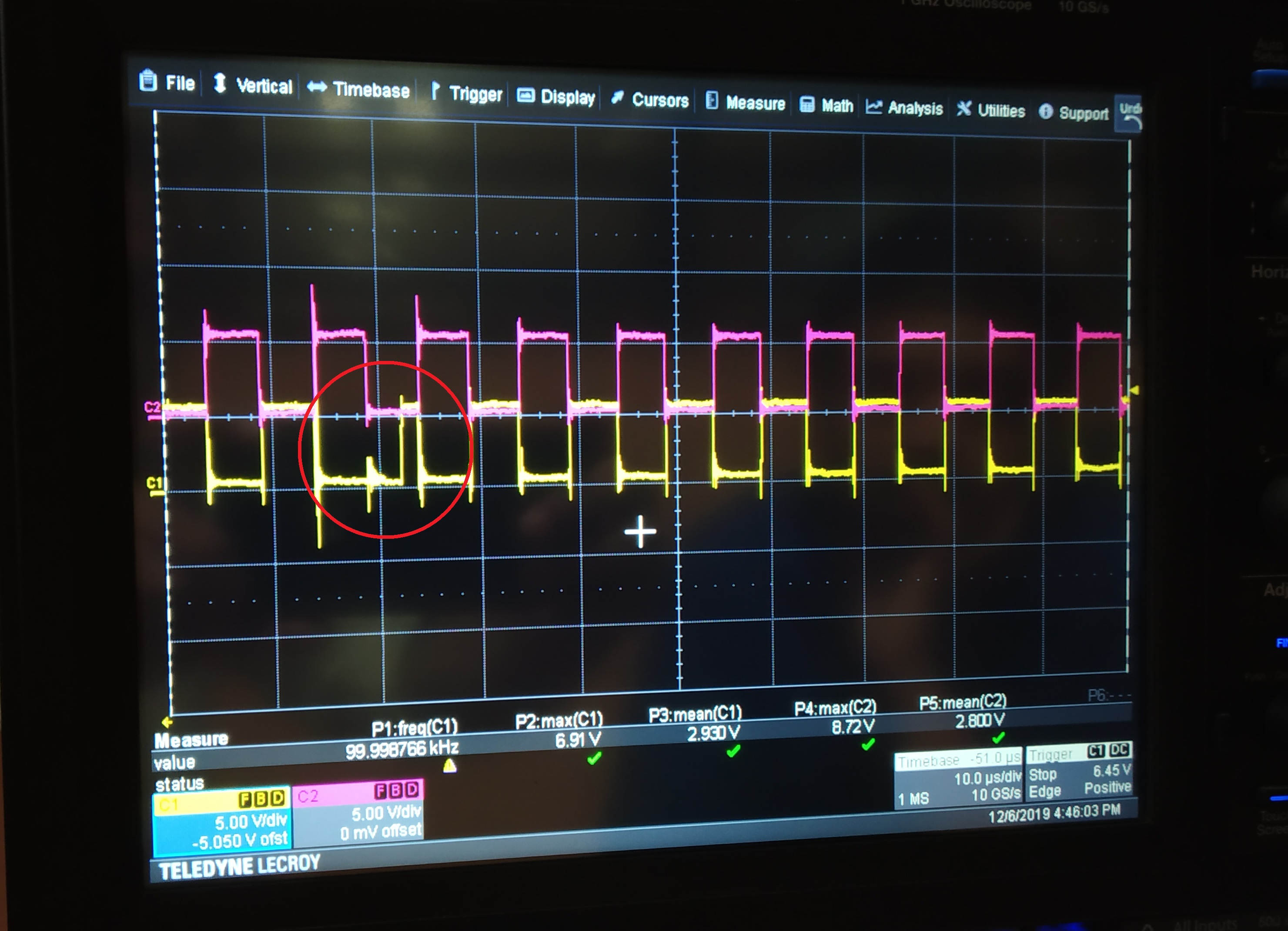
We designed one half bridge module using LMG3410RO70 using the reference from TI. We used it for synchronous boost converter operation. We tested it with open loop configuration. It was working fine when the input voltage is below 30V. But when we increase the voltage above 30V the upper device is not properly switching on and by further increasing 10 more voltage the upper device failed (not getting the 5V from LDO inside the GaN device). Please find the attachment for GaN half bridge schematic and Device voltage waveform. In the wave form you can see that there is a shift in the voltage level during turn on.

  • Hello Jidhun,

    Thanks for contacting us. We will look into the schematics and get back to you in a day. 

    Also is the green signal the input signal?

    Regards,

    Yichi

  • Hello Jidhun,

    This is a follow up on the previous reply. Assuming the green curve is the input signal, then the signal is too noisy with some unintentional turn on due to potential ground bouncing. 

    Looking at the schematics, the TME1212S component should give you the isolation needed. C42, C24, C41, C25 are unnecessary and could be the cause of the ground bounce. Try to remove those 4 caps and see if you have the same problem.

    Regards,

  • Hello Zhang,

    Thank you for the reply.

    The green signal is the input to the LMG3410 and the yellow signal is the voltage across the device. Here the green signal we have measured using single ended probe and the yellow signal is by differential probe.

    But we have tested our system without connecting those capacitors only.

    Regards,

    Jidhun

  • Hello Jidhun,

    If you look at the voltage waveform right before your right circle, it's slightly below the ground level, and the low side FET is likely to be in the third quadrant operation. Third quadrant operation will have ~7V drop, which will generate a lot of loss and heat. The repeating high loss and heat may cause the FET to fail. At the same time, if you look at the corresponding green signal during that time frame, it's low when it supposed to be high.

    Here are some suggestion I have:

    1. Get a thermal couple/thermal camera and monitor the temperature of the FETs. The nominal maximum operating temperature is 125 degree C. If it's overheating, then the device will likely to fail.

    2. Probe input signal from signal generator and IN pin of the device, and check where the signal has abnormal behavior. Check the circuit for input generation for both high side and low side FETs.

    Regards,

  • Hai Zhang,

    Here I am attaching two figures,

    1. Fig. 1 the two pulses, yellow one is the upper device pulse (input to LMG) there you can see the change in pulse.

    2. Fig 2 the LDO voltage of the two devices, there pink one is the upper device voltage and yellow is the lower one. Pink one shows lot of distortion

    What may be the reason ?

  • Hello Jidhun,

    1. For the input signal, from the original figure, it seems like that the low side FET signal has abnormal behavior. In this post you said it's the high side signal has this behavior. Could you clarify this? 

    Like I mentioned in the previous post, you might want to probe the IN signal along the path: before the isolator and after the isolator. If this happens before isolator, then it's the problem with the signal generated from the motherboard; if the signal is normal before the isolator, but act abnormally after the isolator, then it will be the isolator problem.

    2. For the LDO signals, it seems that the pink signal is stepping up and down. Since the current go through it will only be a couple mA and there's a capacitor connected with LDO, it should not happen. It's most likely to be a measurement problem. Please check the differential probe you are using.

    Regards,

    Yichi

  • Dear Yichi,

    1. We are having problem in high side FET only. You can see that the pulse is not properly switching.

    2. You can see that the LDO voltage from high side FET (the pink one in second figure ) showing stepping up and down. But the low side FET LDO voltage is stable (the yellow one in second fig.)

    Both measurement we have done it using differential probe only.

    This pulse distortion is happening only after the isolator.

    Regards

  • Hello Jidhun,

    I recommend you try the following:

    Try to have 0 bus voltage and probe the IN pin and LDO.

    • If you still have the same problem:

    Try to replace ISO7831 and/or LMG3410 part and test again.

    • If you don't have the same problem at 0 bus voltage,

    Replace the TME1212S part with MEJ1S1212SC. Datasheet here. The converter you are currently using has too large isolation capacitor (60pF) and may cause ground bounce.

    Thanks,

  • Hello Yichi,

    • At 0 bus voltage all signals are fine.
    • When the bus voltage is above 30V, the signal is getting distorted.
    • The below figure shows the input pulse (yellow one) of the upper device and the fault signal (pink one). Here we are getting a fault signal when input voltage is greater than 30V. What may be the possible reasons for getting a fault signal like this ?

  • Hello Jidhun,

    There are three possibilities that can trigger the fault: over current, over temperature and UVLO. In this case, it's most likely the UVLO is triggered. Again, it could be the ground bounce issue I mentioned earlier causing the upper device not getting the voltages required. Have you tried to replace the DC regulator TME1212S with MEJ1S1212SC?

    Regards,

    Yichi

  • Dear Yichi,

    We have tested our system with the suggested part number (MEJ1S1212SC) but again the same issue exists.

    Regards,

    Jidhun

  • Hello Jidhun,

    Could you please share the layout near the high side GaN? The parasitic inductance and capacitance from the PCB could also cause undesired noises if the layout is not optimized.

    Regards,

  • Hello Yichi,

    Please find the attached layout file for your reference. Kindly verify it.Layout of Half bridge GaN Module.pdf

    Regards,

    Jidhun

  • Hello Jidun,

    The layout has several issues leading to the noise at the high side PWM:

    • (Primary reason for the noise) There is no shielding polygon (connecting to Vsw)under high side device and its surrounding R/C/L. The high side PWM has large ground return path from Vsw of GaN to Vsw to the isolator.
    • Under high side GaN, there is a polygon connecting to the power ground, not high side signal ground. The polygon cannot help with the signal shielding but add CM noise into the low side signal.
    • Please refer to our EVM on our website as a layout guideline.

    Regards,