


Hi TI support engineer,
Thanks for your look at this issue.
We used BQ25890 to charge a 3.7 V battery, its charge complete voltage is 4.2 V.
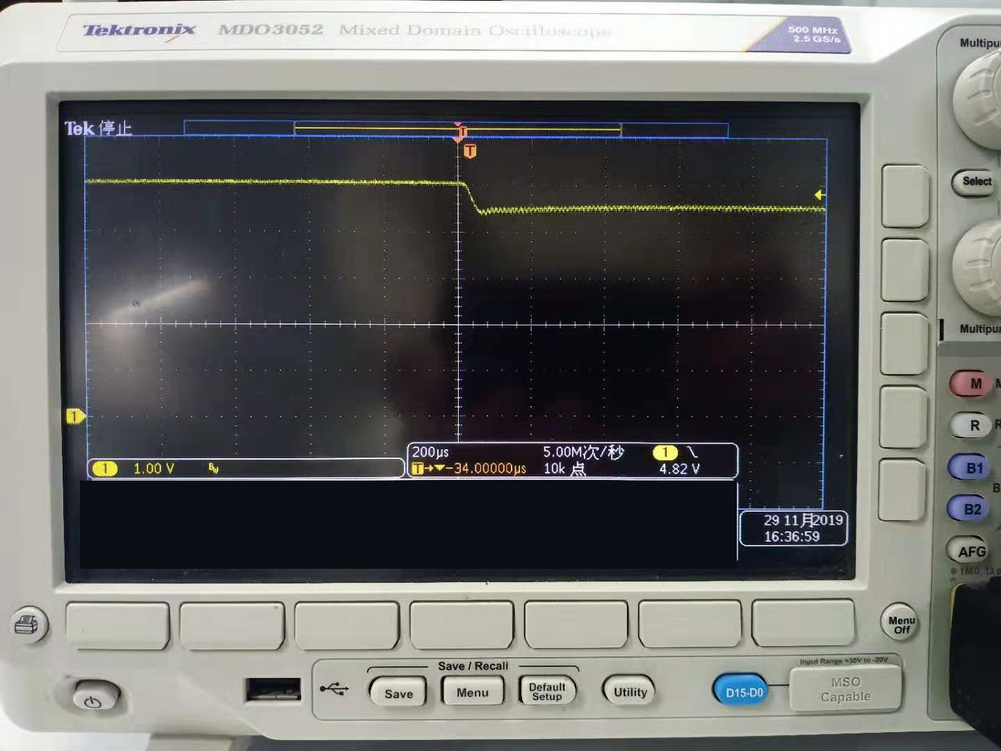
When charge closing to complete (battery voltage almost 4.2 V), after we removal Vbus attached to BQ25890's VBUS pin, there have a chance that the BQ25890 will reverse output a weak 4.4 V to VBUS pin (the charge more close to complete, the issue's appear chance is grater), that cause BQ25890 don't know the VBUS was removal, and won't generate an interrupt to tell our system's CPU, and CPU won't send charge disable command to BQ25890, so the BQ25890 stay in this weak reverse boost state, sometimes this state will last about 5 seconds, sometimes this state will last forever. The Vbus wave form as below:
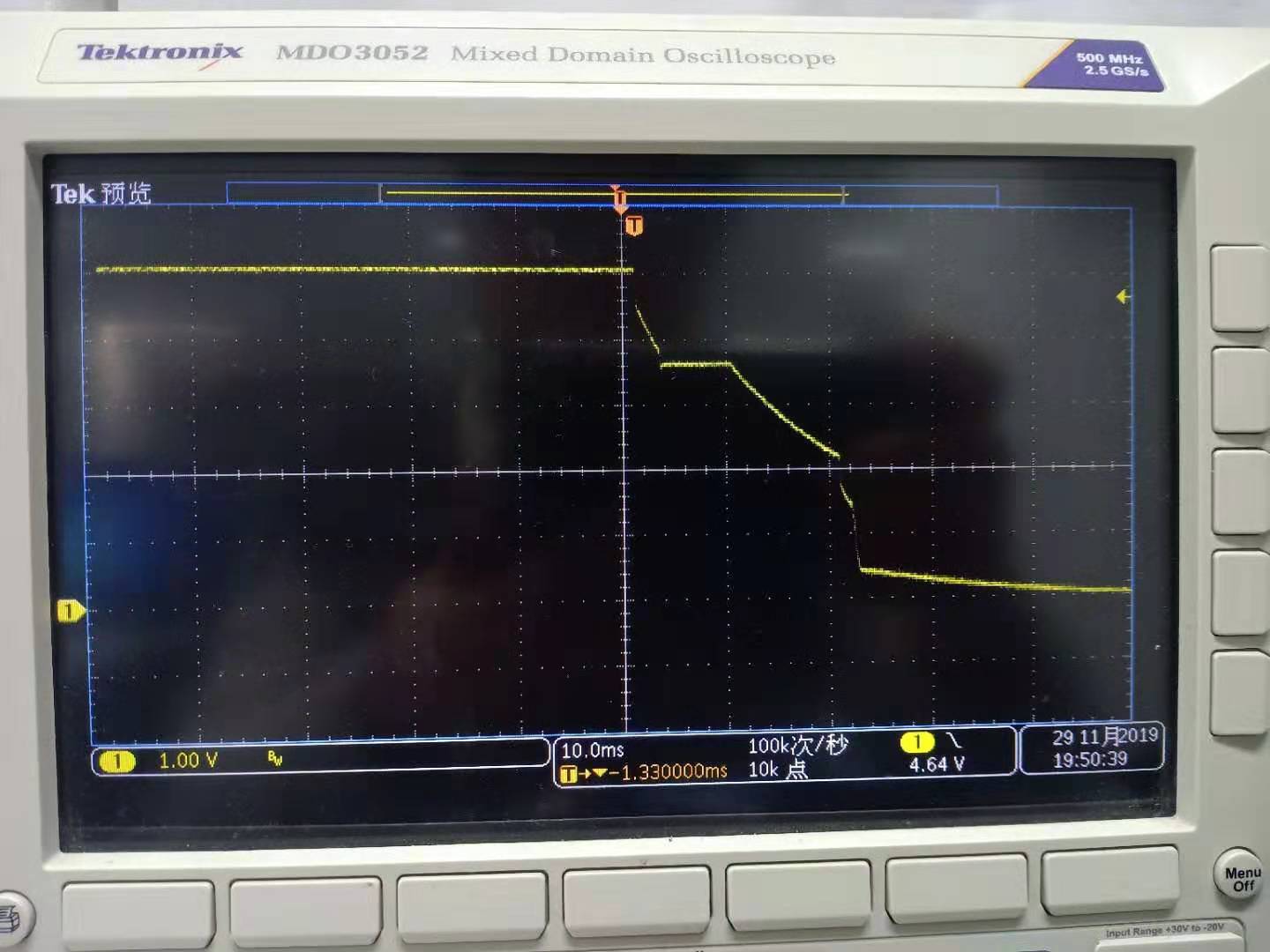
Sometimes hadn't appear this issue, after VBUS removal, we can see the VBUS also not drop directly, the wave form as below:
In that abnormal state, I measured BQ25890's OTG pin, it's low, and its "SW" pin have switching wave form, so the 4.4 V voltage should be reverse boost by BQ25890, but not controlled by OTG PIN.
The output 4.4V is weak, when we add some interfere to VBUS pin, like use an electronic load to sink 1 mA current, the 4.4 V will disappear immediately, and BQ25890 will generate an interrupt output by INT pin, and quit this abnormal state.
The abnormal reverse output voltage will follow VINDPM setting change to change, after we change VINDPM to 4.5 V, the VBUS abnormal reverse output voltage will be 4.5 V, and set VINDPM to 4.6V, the VBUS abnormal reverse output voltage will be 4.6 V. But when we set VINDPM to 4.7 V, this abnormal state will not appear, seems all is OK.
I think it's should be when charging current very low, after remove attached VBUS, before the VBUS drop to the voltage level that can generate a Vbus removal event in BQ25890, because BQ25890's switching works continually, it boost battery's power reverse to VBUS, and BQ25890 don't know it, BQ25890 treat this 4.4 V Vbus as input power supply, so it stay in charging state, but it's not charging actually.
In charging, before removal attached VBUS, the BQ25890's register setting are:
bq25890 REG 0 = 0x7f
bq25890 REG 1 = 0x6
bq25890 REG 2 = 0x5d
bq25890 REG 3 = 0x1c
bq25890 REG 4 = 0x20
bq25890 REG 5 = 0x11
bq25890 REG 6 = 0x5e
bq25890 REG 7 = 0x8d
bq25890 REG 8 = 0x3
bq25890 REG 9 = 0x44
bq25890 REG A = 0x71
bq25890 REG B = 0x76
bq25890 REG C = 0x0
bq25890 REG D = 0x13
bq25890 REG E = 0x5f
bq25890 REG F = 0x5f
bq25890 REG 10 = 0x3f
bq25890 REG 11 = 0x98
bq25890 REG 12 = 0x4
bq25890 REG 13 = 0x7f
bq25890 REG 14 = 0x5d
After removal attached Vbus, this issue appeared, the register are:
bq25890 REG 0 = 0x7f
bq25890 REG 1 = 0x6
bq25890 REG 2 = 0xdd
bq25890 REG 3 = 0x1c
bq25890 REG 4 = 0x20
bq25890 REG 5 = 0x11
bq25890 REG 6 = 0x5e
bq25890 REG 7 = 0x8d
bq25890 REG 8 = 0x3
bq25890 REG 9 = 0x44
bq25890 REG A = 0x71
bq25890 REG B = 0x76
bq25890 REG C = 0x0
bq25890 REG D = 0x13
bq25890 REG E = 0x5c
bq25890 REG F = 0x5c
bq25890 REG 10 = 0x3f
bq25890 REG 11 = 0x93
bq25890 REG 12 = 0x0
bq25890 REG 13 = 0xbf
bq25890 REG 14 = 0x5d
And then attached VBUS again, the register are:
bq25890 REG 0 = 0x7f
bq25890 REG 1 = 0x6
bq25890 REG 2 = 0xdd
bq25890 REG 3 = 0x1c
bq25890 REG 4 = 0x20
bq25890 REG 5 = 0x11
bq25890 REG 6 = 0x5e
bq25890 REG 7 = 0x8d
bq25890 REG 8 = 0x3
bq25890 REG 9 = 0x44
bq25890 REG A = 0x71
bq25890 REG B = 0x76
bq25890 REG C = 0x0
bq25890 REG D = 0x13
bq25890 REG E = 0x5f
bq25890 REG F = 0x5f
bq25890 REG 10 = 0x3f
bq25890 REG 11 = 0x98
bq25890 REG 12 = 0x5
bq25890 REG 13 = 0x7f
bq25890 REG 14 = 0x5d
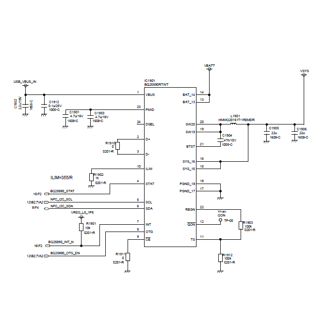
Our schematic as below:
Help to confirm whether you had encountered this issue before? And whether there have some design errors in our schematic caused this issue? How can I to resolve this problem?
Thanks for your help.
Michael Smith.
