This thread has been locked.

If you have a related question, please click the "Ask a related question" button in the top right corner. The newly created question will be automatically linked to this question.

BQ4050: External Cell Balancing : which is correct circuit?

Part Number: BQ4050
Other Parts Discussed in Thread: BQ40Z50

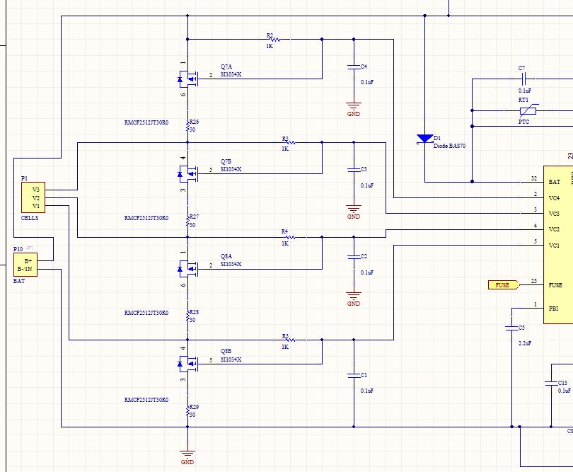
Need clarification on circuit for BQ4050 and external FETs for cell balancing. BQ4050 Datasheet refers SLUA420A for details, but said document is not compatible or usable with BQ4050. Found a thread .. e2e.ti.com/.../342036 Here is detail on the BQ40Z50 ... not quite the 4050, but answers provided are conflicting. I have chosen the solution as per this link... e2e.ti.com/.../Ext.-Balance.JPG However further discussion would indicate that this solution may not work and a proposed schematic using P channel and N fets is the correct solution. However, as discussed that solution required a firmware update in the BQ40Z50 to work ... which is not available as far as my understanding goes, with the standard BQ4050. Hence I need clarification as to what circuit is correct.


  • Allow me to double check and then provide my feedback. Thanks.

  • Dear Andy. Much appreciated. Was hoping to have an answer by now. Any chance we might have answers today 2019-12-06, as it is urgent please.

  • Hello Ulrich,

    Sorry for my late response. I'm looking into your question now and will reply to you by the end of today. Thanks.

    Andy

  • Hello Ulrich,

    My colleague who is an expert on the device has not replied to me yet.  Allow me to provide our answers tomorrow morning.  

    Andy

  • Verry sorry for our late response. Both Thomas and Simon left our group years ago and therefore we had to turn to other experts for help.

    BQ4050 and BQ40z50 share very similar designs and therefore we believe that Thomas's suggestions can be applied to BQ4050 as well. We would suggest you follow his recommended circuits.

    The P-CH will work as it is off normally with the gate pulled up to the VC1 cell voltage. When the VC1 to Vss CB bypass FET is turned on the PCH will be turned ON and the CB current will flow.

    The P-CH benefit over the N-CH is the predictability of the RDS(on) of the FET and hence the accuracy of the calculation of the CB bypass FET ON Time. Using an NCH in the VC1-VSS case will provide a limited VGS and could vary so that the FET could be in the linear region and hence its RDS(on) is not stable for the purposes of calculating the CB bypass on time. The P-CH version will be a solid ON and therefore more predictable. The outcome is essential that the balancing of Cell 1 could take longer than expected when using an NCH.

  • Dear Andy. Thank you so much for the feedback and confirmation. Much appreciated.