This thread has been locked.

If you have a related question, please click the "Ask a related question" button in the top right corner. The newly created question will be automatically linked to this question.

LM25116: PCB review

Part Number: LM25116

Hi,

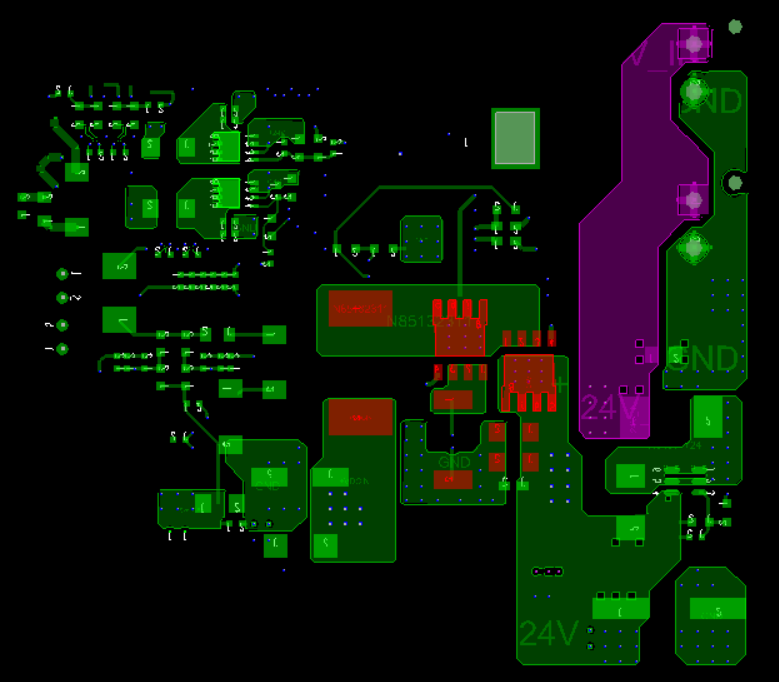
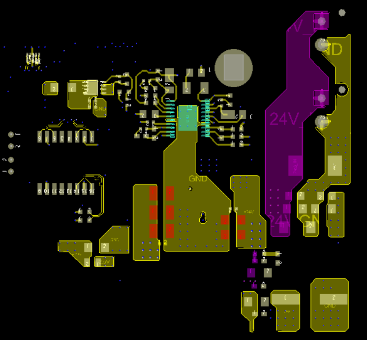
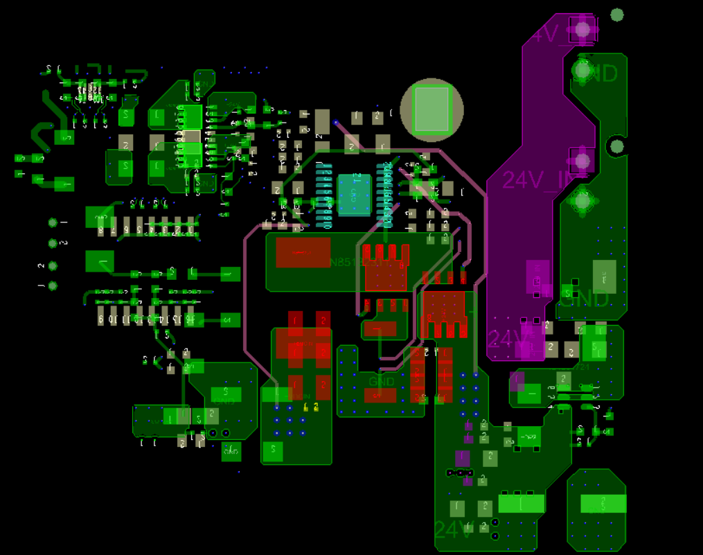
Please help to review this PCB. This is a 10 layer design, but only keep LM25116 related . my customer put the device on bottom layer, but put FETs at the top layer. I can't tell if this may cause some problems. please experts help on this. thanks. 

https://e2e.ti.com/cfs-file/__key/communityserver-discussions-components-files/196/sch_2B00_pcb.7z

  • Looking at the schematic, I do not see anything out of the ordinary.

    Please be sure to check your design against Webench and/or any calculator tools that are available for 

    this device on the product folder.

    I can not read the PCB file.  If possible can you convert to Altium or send PDFs of the relevant layout.

  • Hi Frank

    This is a urgent case, No schematic check need, I've done. just help me out the PCB layout question below , thanks. 

    "my customer put the device on bottom layer, but put FETs at the top layer. I can't tell if this may cause some problems."

    you can use below free viewer to open this PCB.

    Download Allegro Free Physical Viewer 17.2

    free tool is limited to turn to pdf, Just put some screenshots here:

    top layer:

    bottom layer:

    mix:

  • I do not think that it is a good idea to put the FETs and controller on different sides of the board.

    The inductance of the connections through the vias may cause some issues.