This thread has been locked.

If you have a related question, please click the "Ask a related question" button in the top right corner. The newly created question will be automatically linked to this question.

LM5145: Circuit and Evaluation Kit Questions

Part Number: LM5145

Hello,

We are working on a design with the LM5145 and had some questions:

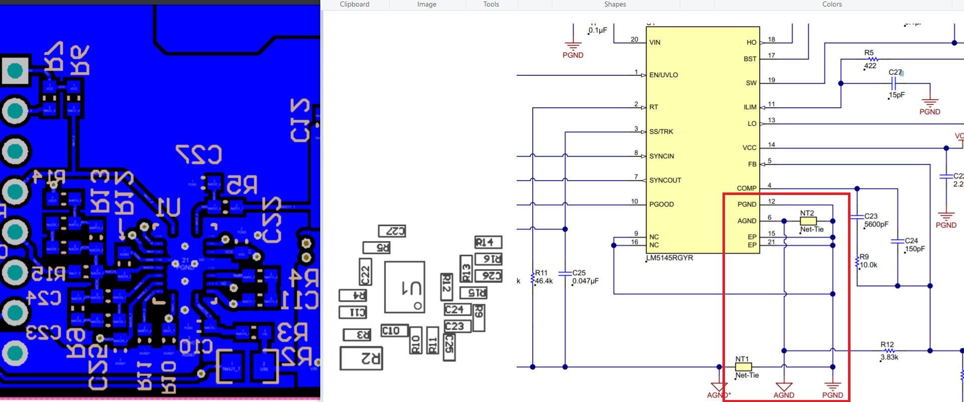
  1. Why are 2 net ties shown in the eval kit schematic, but not seeing them on the Eval Kit PCB?
  2. Why are “NC” (no connect) pins connected to GND on Eval Kit?
  3. Are pin 12 PGND and pin 6 AGND tied together inside the IC? Block diagram indicates AGND and PGND are completely separate.
  4. In functional diagram figure 8.2, I’m not seeing a pin for Thermal Tab under IC. Eval Kit ties PGND and AGND under the IC.
  5. The max current from 7V reg for logic supply is called out as 40mA min. Is this capable of delivering 40 mA to other circuits, or do we need to account for the IC quiescent current as well in this number?

Thank you, Keith

  • 1. The net ties may be hard to see; they are just shorts in the metal

    2. We typically connect the N/C pins to ground for convenience and to help with thermals.

    3. The ground pins are connected softly inside the device.

    4. The DAP must always be connected to ground.

    5. The 40mA is the short circuit current.  It is stated so that if a short occurs on that pin, the maximum current is known.

         I would not VCC as a logic supply.