This thread has been locked.

If you have a related question, please click the "Ask a related question" button in the top right corner. The newly created question will be automatically linked to this question.

WEBENCH® Tools/LM5005: LM5005

Part Number: LM5005

Tool/software: WEBENCH® Design Tools

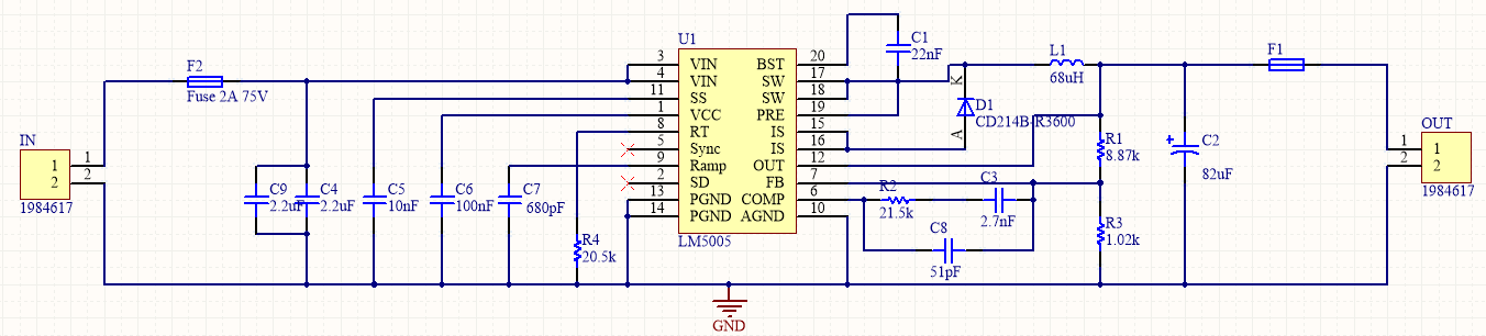
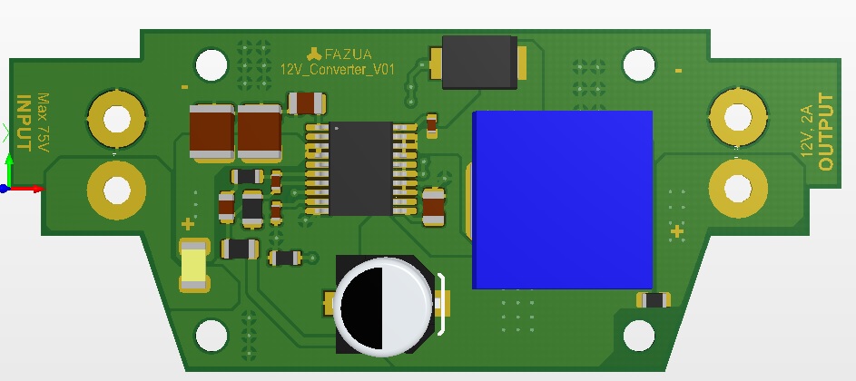
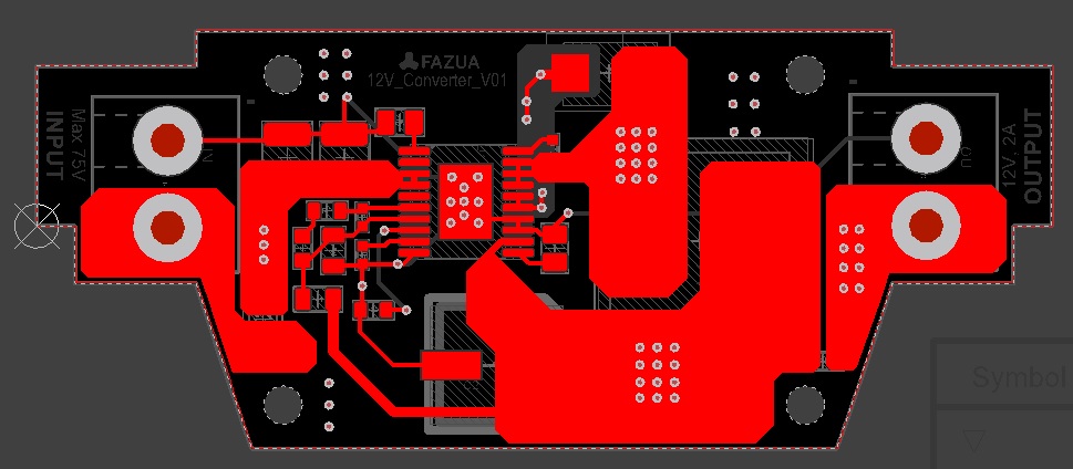
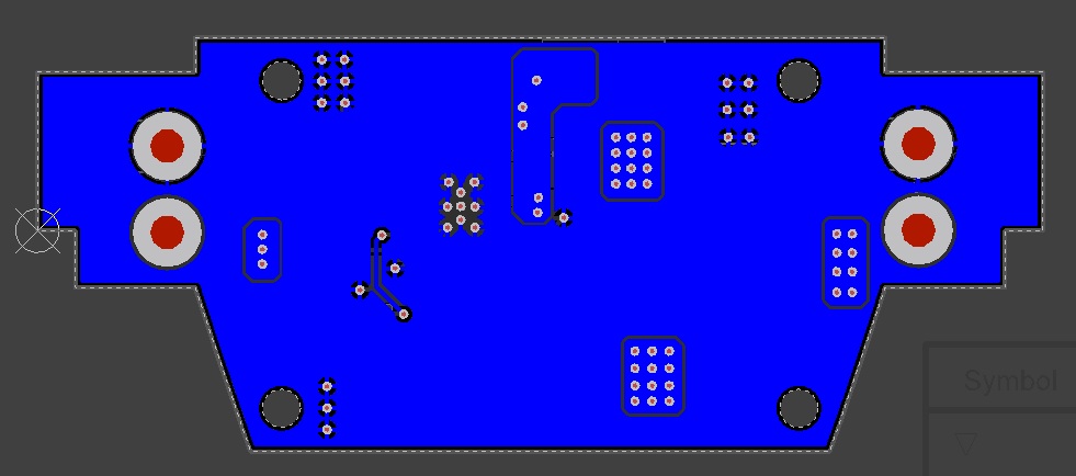
I have designed a DC/DC converter using LM5005 and based on TI Webench tool. My designing criteria is INPUT: 30-75V, OUTPUT: 12V,2Amps. After producing and testing sample PCB. The LM5005 burned at 300mAmps!!! I have few questions: 1- why it happened? 2- Is it possible to open a case and explore the problem? 3- what is the solution? is there any more reliable alternatives?

Regards,

Jafar

  • Jafar, 

    There are many different possibilities for a blow up, can you start by sharing your schematic with me?

    Was the output voltage correct at no-load? 

    -Orlando

  • Thanks Orlando, Yes the output was OK at no-load. Here is my schematic. thanks for the feedback.

  • Jafar,

    Your schematic looks OK, are you able to share your layout with me?

  • Dear Orlando, 

    Thank you and happy new year.

  • Jafar,

    I just noticed you only have an electrolytic capacitor on your output.

    We recommend having a low ESR ceramic output capacitor to minimize output voltage ripple, generally a combination of ceramic+electrolytic output capacitor are used.

    The electrolytic has significant ESR which leads to significant output voltage ripple, and I think that is the root cause of your failure.  

    The LM5005 is trying to respond fast to the voltage ripple swings, and with significant swings this can lead to instability.

    Can you record some oscilloscope waveforms for me at no load? Also lightly loaded (~100mA) would be great. 

    I would like to see SW node voltage and Vout ripple.

    If I am correct about the issue we can slow down the response speed of the converter to account for this large output ripple voltage.

    Another potential issue is the inductor, please be sure your inductor saturation current is above the current limit of the part (3.5A typ, 4.25A MAX). 

    Other feedback on the layout:

    The loop between SW-Inductor-Diode-IS should be kept on the same plane and not routed through vias. See the example layout in section 10.2 of the datasheet.

    I look forward to those waveforms,

    -Orlando

  • dear Orlando,

    Thanks for the comments.

    I have designed based on TI WEBENCH, I have used the exact components recommended by WEBENCH. The Inductor saturation current is above the current limit of the part. 

    I see a small output voltage ripple. please see the photos below:

    Another point that I would like to point out is that the IC gets heated so much, the IC and inductor temperature in 200mA load is about 80C!!

    We are planning for 60000 PCs for next year's production. I hope with your help I can solve the problem.

    Regards,

    Jafar

  • Jafar,

    Your output ripple is good, the converter looks stable and it is probably not the output capacitance causing the issue.

    It appears your vias under the ICs exposed pad are not connected to the GND planes.

    These vias are necessary to move heat from the IC to the PCB to prevent the LM5005 from overheating.

    From the pin description in the datasheet: "Exposed pad. Exposed metal pad on the underside of the device. Connect this pad to the PCB ground plane to assist with heat spreading."

    You should pour GND to the vias under the IC on ALL layers for best heat spreading. Use solid pour around the via for maximum copper and heat conductance.

    That should fix your IC overheating, however, I'm not entirely sure why the inductor would be heating up to 80C too.

    Maybe it's the IC spreading heat to the inductor through SW, or maybe the DCR is too high. 

    If your inductor still overheating after fixing the exposed pad, I would try an inductor with lower DCR.

    Hope this helps,

    -Orlando

  • Hello Orlando,

    Thanks for the comments, but the vias under the IC are connected to the GND polygons. The PCB gets heated as well as the IC and inductor. The PCB is a 2 layer PCB. I even used a heatsink connected (using silicon pad) to my board but it didn't work as well. please see screenshots top and bottom layers of the IC:

    Regards,

    Jafar

  • Jafar,

    The top layer copper is not filled solid pour, you have necks that limit the thermal spreading to only 4 traces, and realistically only two of them are connected to enough copper to absorb the heat.

    You should fill the GND planes solid as you did with SW, ISEN and VOUT polygons. That will definitely help spread the heat accumulating within the IC to the PCB and lower your temperatures.

    -Orlando