Tool/software: WEBENCH® Design Tools
Hi guys ,
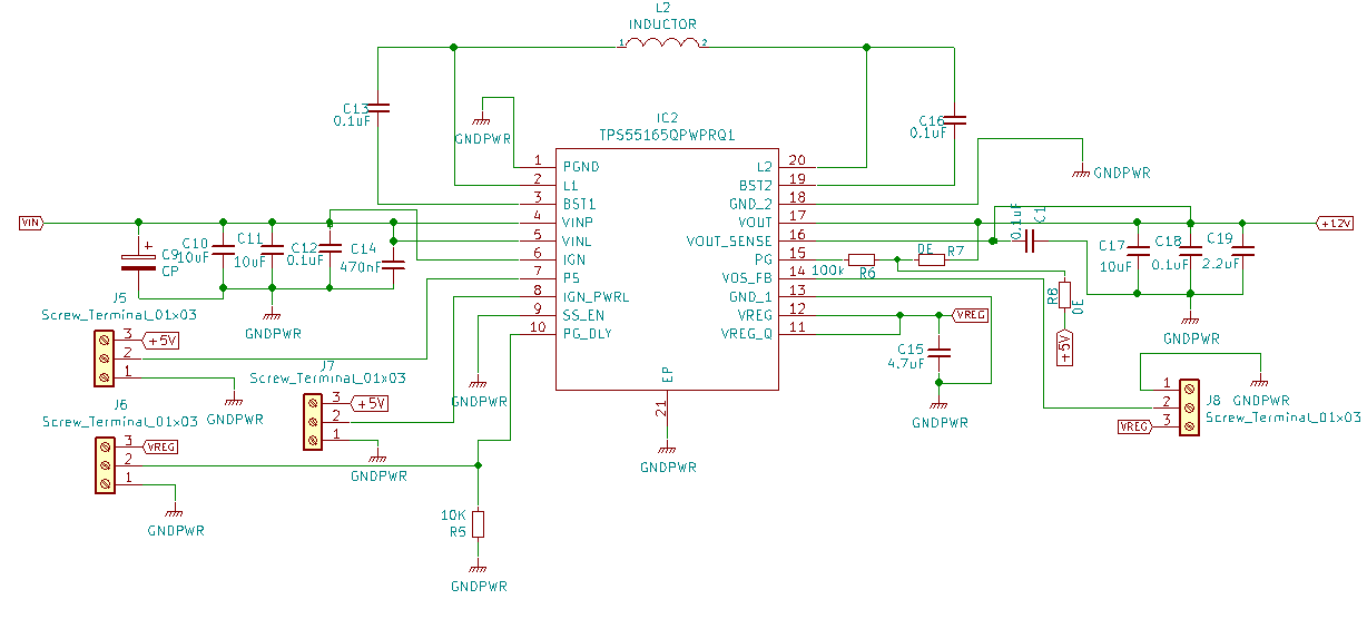
configuration of pins like web bench design
VINP ,VINL,IGN - Input supply
IGN _PWRL,PS,SS_EN,PG_DLY - GND
VOUT _SENCE - 10uF to Vout
PG - 100K to Vout
VREG,VREG_Q,VSOP_FB - Connect with 4.7uF cap to gnd
but it's not responding , I don't know why?
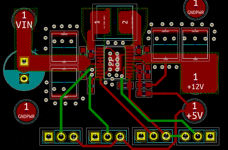
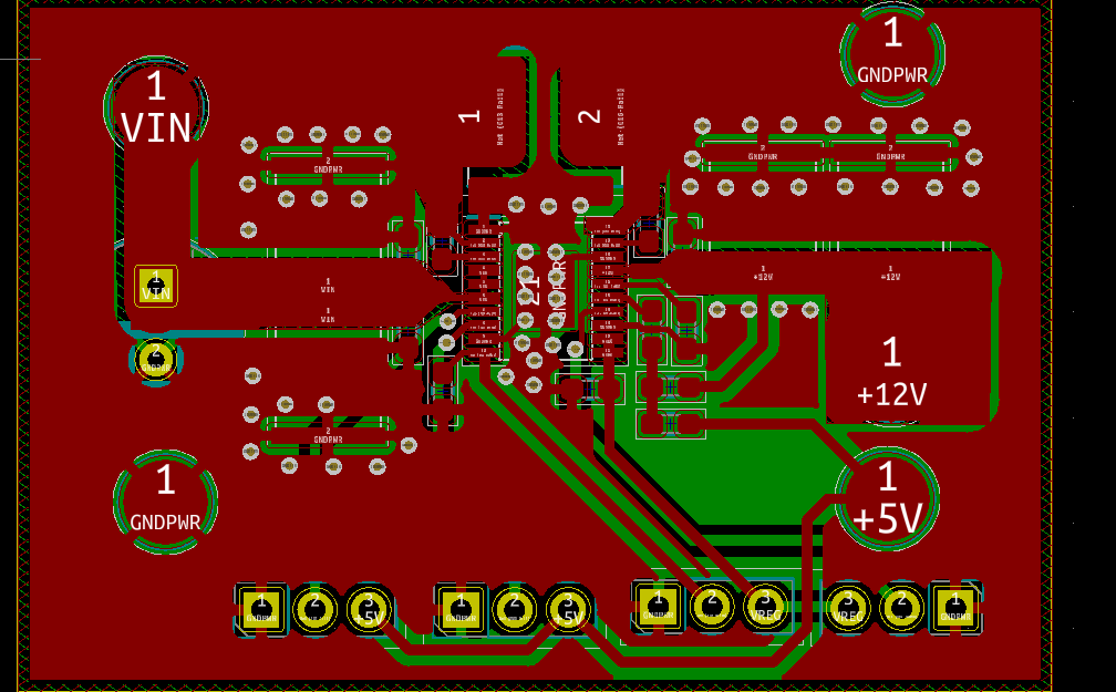
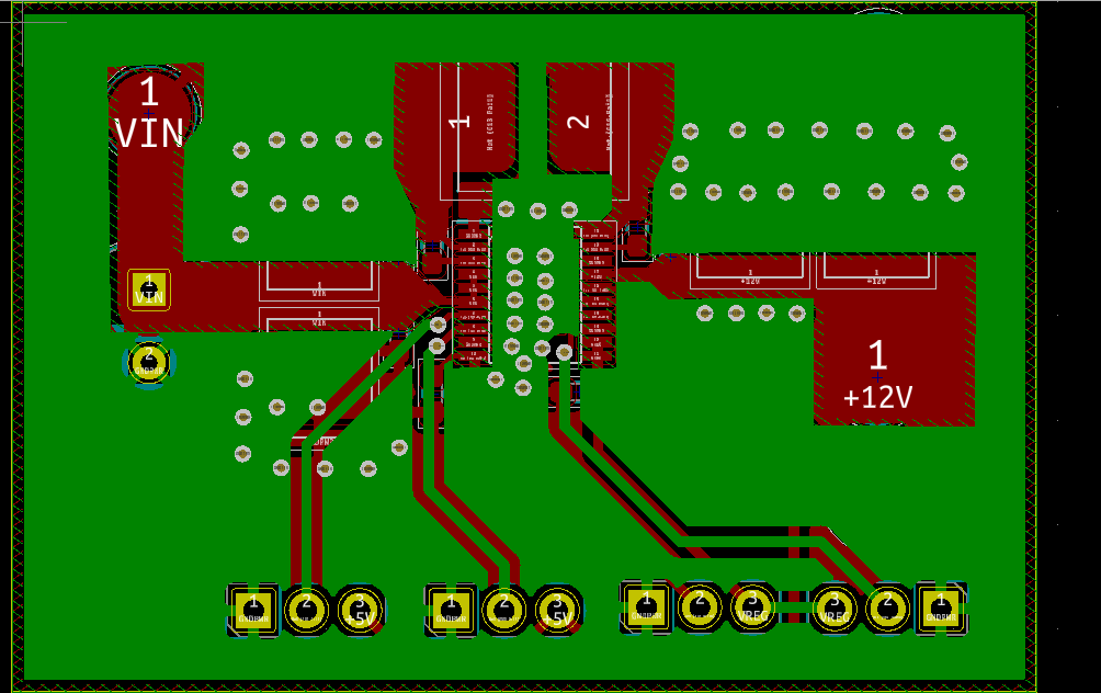
and I am attached my layout for new board is this ok for next revision ?
is there any other config for this circuit ?
the attached layout 2 layer bottom fully gnd ,top also fully gnd and also please check component placements