This thread has been locked.

If you have a related question, please click the "Ask a related question" button in the top right corner. The newly created question will be automatically linked to this question.

BQ25895: BQ25895 query

Part Number: BQ25895

HI

We design with BQ25895, use non-standard adapter as input, one output charge the battery, another output to OTG to power the peripherals.

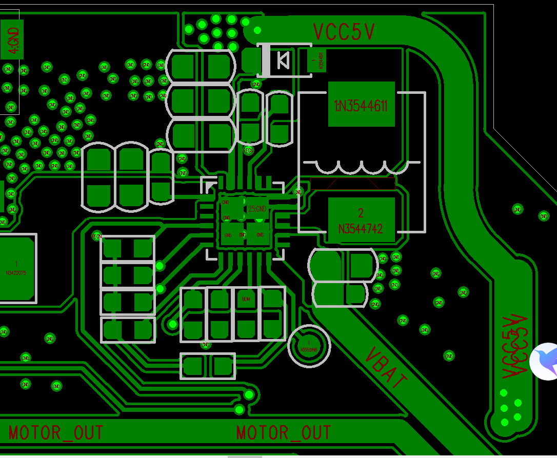
When there is no adapter, the battery power is boosted to OTG to power the peripherals at the same time, such as the schematic diagram of the accessory and the pcb diagram. In the current debugging, the maximum input current limit is set to 3.25A.

ILIM  pin connect to 100ohm, the constant current charging current is set to 2A. D + D- Detection function is disabled. Register settings are as follows:

REG00:0x3F
REG01:0x06
REG03:0x3A
REG04:0x32
REG05:0x13
REG06:0x5E
REG07:0x89

other registers use default setting

1. Connect the adapter to charge, when the battery is 3.6v, the charging current is about 700ma

2. Without the battery, just plug in the adapter. When the OTG output is connected to the load 1A, the voltage output of the OTG is 4.97V (input voltage is 5.12V). When connected to 2A, the output voltage is 4.67V (input voltage is 5v) and the output is 3A.

When the output voltage is 4.2V (the input voltage is 4.8V). According to the description in the specification, the internal resistance of the RBFET is 38mohm, but the actual test is 200Ω (3A)

3. Only connect battery, OTG output is connected to 3A load, OTG output voltage is 4.9V. Attached OTG waveform as below.

7536.bq25895.pdf

OTG  waveform

Waiting for your reply

Thanks

Star

  • Hi Star,

    Regarding 1, I assume you are expecting higher charge current?  If so, what is the voltage measured at VBUS and VBAT pins?  What do the status registers report when charging?

    Regarding 2, I don't understand the statement "plug in the adapter" in OTG mode.  In OTG mode, you cannot have an adapter at VBUS.  If there is an adapter at VBUS, OTG mode is disabled, charge mode is enabled and any load at PMID load gets V(PMID)=V(VBUS)-RBFET*IPMID

    Regarding 3, the waveform shows the OTG output collapsing every 500ms.  Can you retake showing the IOTG current and the SW node?

    Regards,
    Jeff

  • Hi Jeff

    Thanks for your reply.

    The VBAT voltage is 4.2v. 5v input voltage
    The sw switching waveform is as follows. In addition, we set the switching frequency to 1.5MHZ, why the test only 500Khz.

    Thanks

    Star

    VBAT 电压为4.2v。输入电压为5v

  • Star,

    If OTG_CONFIG bit =1, any write to the boost switching frequency bit is ignored.  You have to write to the boost switching frequency bit before enabling OTG boost mode.  Were you able to measure the load current on VBUS during OTG boost mode?  Were you able to capture the status and fault registers?

    Regards,

    Jeff