This thread has been locked.

If you have a related question, please click the "Ask a related question" button in the top right corner. The newly created question will be automatically linked to this question.

TPS562201: High ripple on output

Part Number: TPS562201

Hi,

We've designed a TPS562201 into an existing product, which is about to go into production.The TPS562201 is powering an ESP32-Wroom32 module, from a 12Vdc powersupply (Meanwell IRM-30-12).

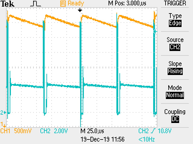
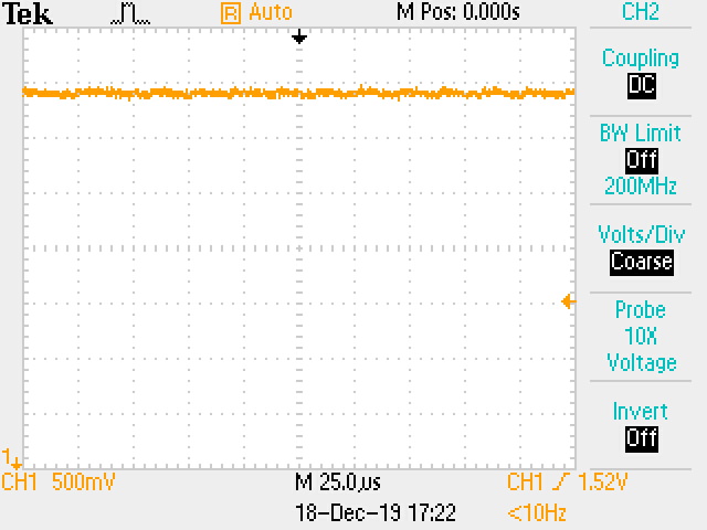
Our initial prototype worked fine. We bought prototype components through Mouser, and the boards worked as expected, 3.3V output from TPS562201 looked good. Then, we purschased a large batch TPS562201 from the TI store, and built 9 boards in a pilot run before running full assembly of 1.000 boards. Now, with the new (9) boards, the ripple out of the TPS562201 is almost 500mVpp. With the ESP32-Wroom32 is running (drawing around 100-150mA), the ripple is complete sawtooth shaped, with a frequency of around 17kHz (see screenshot below).

We did not make any board changes between the prototype and pilot run. The only difference is the TPS562201 coming from 2 different sources (Mouser / TIstore). They're both marked 2201, but the lines on the SOT23 packages (which I suspect are used for revision) are a bit different from the 2 sources.

If the ESP32 module is in standby (drawing less than a mA), the ripple frequency is around 80Hz, still with a sawtooth ripple of around 500mVpp. Output capacitors are 2x22uF, 10V, X5R. The ripple is almost the same shape no matter the amount of current we draw (1mA og 100mA).

What can explain the high ripple? What I find interesting is that the low voltage on the ripple is actually the setpoint (3.3V), while the high voltage (upper peak) is much higher, about 3.7-3.8V. So it seems there's a massive current boost that charges the output capacitors way too high (up to 3.8V), and then the regulator doesn't add any current (charge to the output cap) until it's down to 3.3V again.

This also explains the frequency changing when the current is higher or lower (lower current = lower frequency). We have about 60-70uF on the output. The frequency is about 17kHz or 60us. This means that we would see a drop of 1V pr. 1A, or 400mA = 400mV given the timeframe (60uF vs 60us).. So when we go into standby on the module, we see the drop taking about 12,5ms, which corresponds to a few mA. So the theory of capacitor discharge is proven to work..., but what causes the TPS562201 to overregulate and make the high voltage/current boost to begin with?

We're ofcourse worried about this, and we have a very tight timeframe to solve the problem, massproduction will start soon.

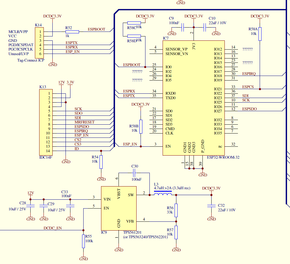
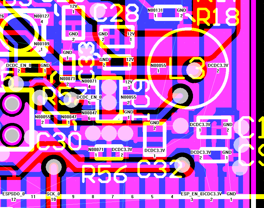
I have attached a snippet of the schematic (partial). C32+C10 are very close on the PCB, so we have a total of 44uF + the internal capacitance in the ESP32-Wroom32, on the output of the TPS562201). The ripple is measured across C32.

Thank you for any pointers or help.

Jacob

(This is showing the ripple voltage on pilot run boards (total of 9 boards, all same behaviour)):

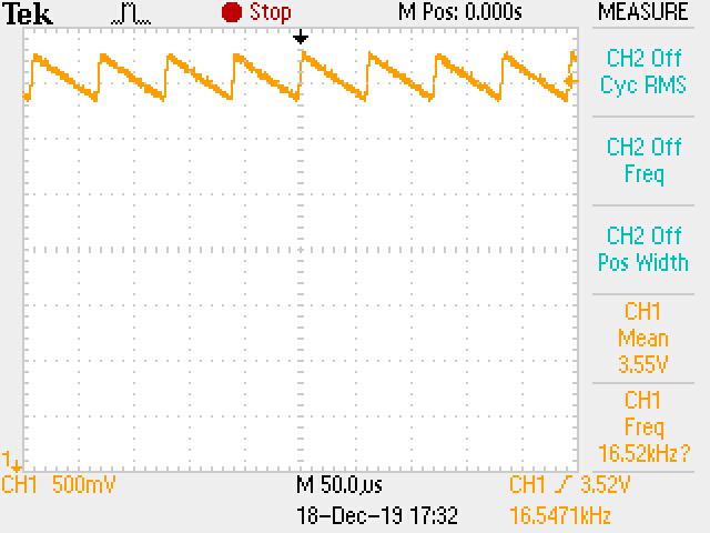
(This one showing the ripple on our initlal prototype board):

(And finally a partial schematic:)

  • Hi,

    There is no issue for the schematic, could you please also share the layout? Let's review it.

    How many boards have this issue? All of them? 

    And have you tried to change another IC to see if there still have this issue?

    You also can try to do the cross experiment, exchanging the IC of the prototype and pilot run board.

    Shawn

  • Thanks for the reply.

    All pilot run boards (9) experience the same problem.  ESP32-Wroom32 is from the same batch on all boards by the way.

    We did try to cross them, but we only have parts left from the prototype (which worked fine) to test on the new pilot run boards. They show the same problem on the pilot run boards, so most likely not related to the parts revisions.

    I have attached a screenshot of the PCB layout:

    It's a 2 layer board, got a bit tight because the wifi module was added to an existing board, with some physical restraints.

    I noticed in the TPS562201 datasheet, in the application schematic, there's a capacitor parallel to the resistor in the feedback loop.  It's not mounted (and not added in my schematic), but is this for stability?

    I'm not sure I'm seeing a stability problem here, though.

    Jacob

  • Hi,

    The layout is not good, R56 is far away from FB pin, the noise is easy to be introduced to FB pin, this would lead to stability issue.

    You can try to move R56 to be close to FB pin, and check if there is improvement.

    Shawn

  • Hi,

    I agree the layout is not perfect, but I wouldn't say R56 is far from the FB pin.  The total trace from R56 to the FB pin is 5mm.  I tried attaching R56 directly onto R57, and made a very short (<10mm) wire from C32 to R56.  No change at all.

    So I made 2 new oscilloscope screenshots, showing exactly what happens on the SW pin compared to the 3.3V output:

    When the output voltage (feedback) is below 3.3V, TPS562201 starts regulating.  The output voltage gets too high, and TPS562201 stops regulating until the voltage is down to 3.3V again.

    Zooming in:

    We get 3 (why 3?) pulses of about 500ns each, which raises the output voltage to about 3.5V.  Now we're already to high.  After the 3 pulses, the lowside mosfet pulls the inductor to ground, releasing the energi in the coil giving a further boost up to 3.75V.  Finally the coil is relased after 3us.

    Around 65us later, the capacitors on the output are discharged to the expected 3.3V and the regulator starts again.

    Best regards

    Jacob

  • Hi Jacob,

    The FB trace is underneath the boot cap, and this trace is connected to FB pin directly, the switching noise is easy to be introduced to FB, that is why I ask you move R56 close to FB pin. If you only attached R56 onto R57, and use a wire to connect C32 and R56, the trace underneath the boot cap is still connected to FB pin, that is why there is no improvement.

    There are two methods:

    1. Keep the changes you made, then cut the trace near R56 to disconnect the trace underneath the boot cap with FB pin.

    2. cut the trace near R56 to disconnect the trace underneath the boot cap with FB pin, then use R57 connect this trace with FB pin.

    Shawn

  • Hi,

    Is there any other question?

    Shawn