This thread has been locked.

If you have a related question, please click the "Ask a related question" button in the top right corner. The newly created question will be automatically linked to this question.

UCC28950: Please check our waveform.

Part Number: UCC28950

Hello

We are developing smps using UCC28950. We maked sample 200 set . but some sets are break down for aging. Almost 20set 

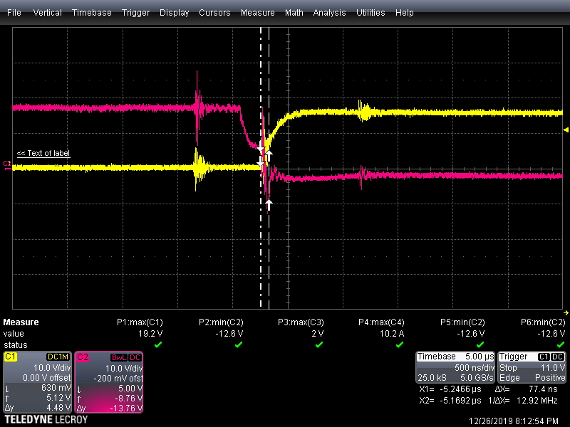
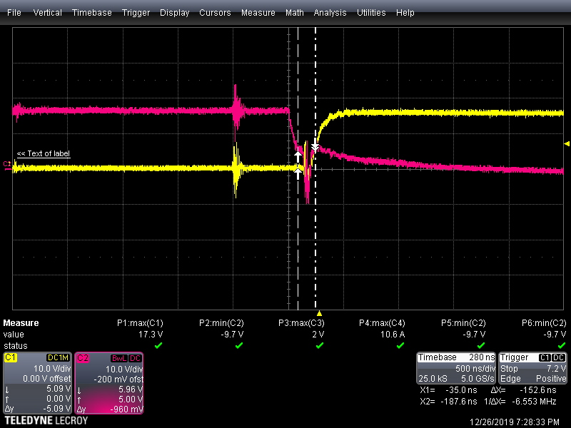
I discovered demaged fet. So plz check some waveform.

I think there are some problem such as no deadtime , current waveform. maybe

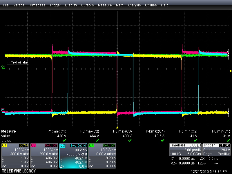
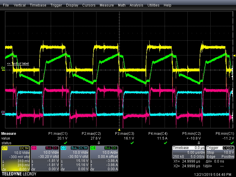
output power : 1.8k  , 53.5V 38A

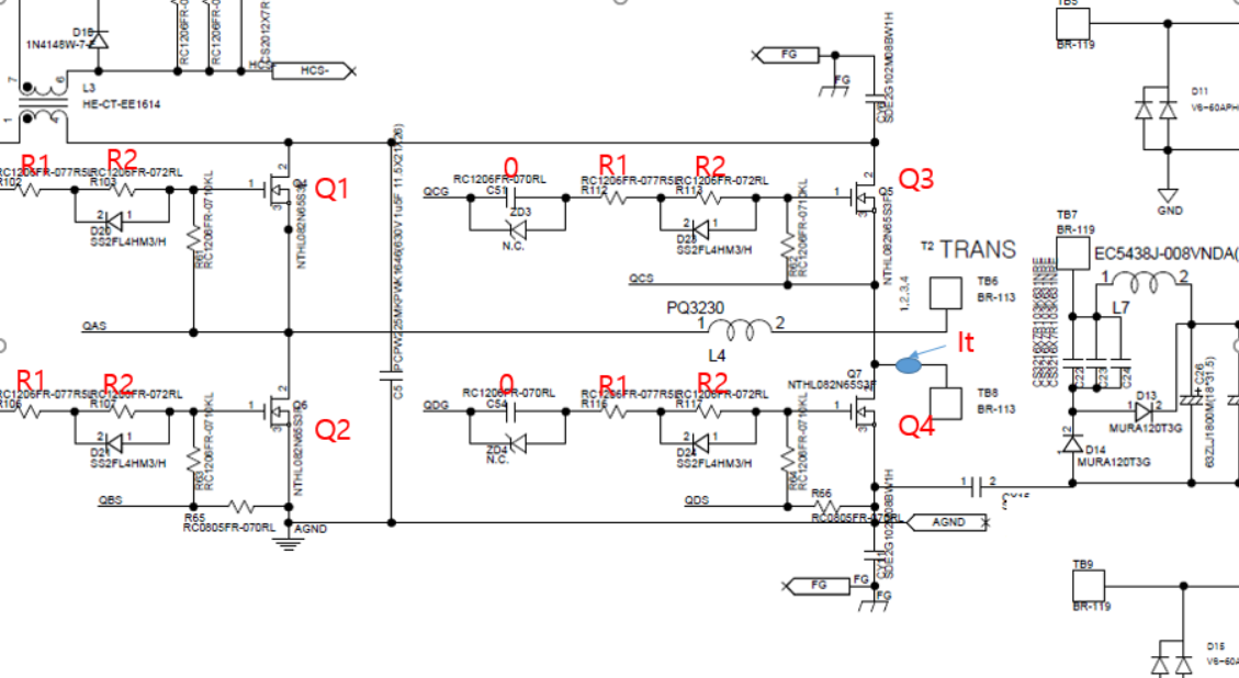
topology : phase shift fullbridge
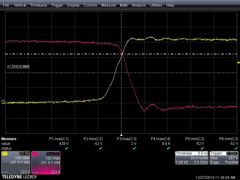
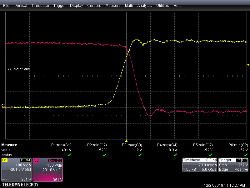
C1: Q2 VDS

C2: Q1 VDS

C3: Q2 Vgs

C4: It  transformer current.

thankyou

  • Hello Kyeongmin

    1/ The VDS waveforms look ok. As the voltage across Q2 increases, the voltage across Q1 must decrease at the same time -

    2/ The delays are between the gate drive signals. To see them you must compare OUTA with OUTB and OUTC with OUTD. These delays will also be present at the MOSFET gates, but not at the MOSFET drains.

    3/ The system is achieving ZVS in the screenshot because there is no Miller Plateau on the gate drive signal for Q2. You should check the Vgs waveforms for the other MOSFETs in the bridge too. However, if the system loses ZVS the efficiency will drop and the MOSFET temperatures will increase.

    4/ You have not included the clamp diodes between the shim inductor L4 and the power rails. These diodes clamp the primary of the transformer to the rails and significantly reduce the voltage spikes seen at the drains of the secondary SRs. This is the first thing I would suggest you check because the voltage spikes can be high enough to avalanche the SR and cause it to fail.

    Please let us know how you get on

    Regards

    Colin

  • Thank you for your reply.

    Your answer is correct. But Vgs is worse than Vds. I think

    This is our waveform. All switch waveforms have spike voltage at  each switching. excluding Q2.  Three switch's Vgs are over maxium rating. especially light load.

    That's why our several set broken , FET and gate driver. 

    I am wondering why Q2 hasn't spike voltage vgs, vds ?  We can get clean vgs vds waveform after adding clamp diode?

    We don't use SR but rectifier. I think this concern also affect into secondary rectifier as well? correct?

    if there is another concern relate to waveforms. plz let me know.

    #1

    c1 : Q4 Vds

    c2 : Q2 Vds

    c3: Q3  Vds

    #2

    c1 : Q4 Vgs

    c2 : Q1 Vgs

    c3: Q2  Vgs

    c3 :It

  • Hello Kyeongmin

    High voltage spikes like this are usually due to measurement, grounding or PCB layout issues. Please re-check the waveforms using a 'tip and barrel' measurement just to get a better measurement of the actual amplitude.

    I'd suggest you look at the PCB layout around Q2 and the other MOSFETs and see if there are differences in the grounding arrangements. If you wish, you can send me your layout (Gerber or original files please) and I'll review it - my email address is 

    colingillmor@ti.com

    The secondary diode voltages can also be affected by high amplitude voltage spikes in the same way as the primary waveforms you show here.

    Please let  me know how you get on - please note I'll be taking time off for Christmas and the New year but if you can send me the layouts today I can review them tomorrow - BTW: I'm based in Ireland so I'm on GMT.

  • Hello

    We resolve our concern.  Our sets is  not damaged anymore. I try to change gate resistor. ( reducing resistor value)

    before: R1 12ohm  R2 0.1 ohm   now : R1 7.5 ohm  R2 2ohm     R1+R2 ==>rising time  // R1 ==> falling time

    I think rising and falling time is faster than before.  So dead time is to longer.  is it correct?. What are you think about our solution?

    Previous sample is damaged by dead time. ( = Fet is shorted  by highside and lowside ' gate turn on simutaneously.)   

    Could you please tell me any recommendation?

    I attched file in terms of  fet switching waveform.

    Previous sample Vgs Dead time : 77ns  (highside , lowside Vgs waveform)
    renewal sample Vgs  Dead time : 152ns(highside , lowside Vgs waveform)
    Previous sample Dead time is shorter than renewal sample.  this waveform is Vds.
    previous  (highside , lowside Vds waveform)
    renewal sample (highside , lowside Vds waveform)
    circuit
  • Hello Kyeongmin

    I'm glad to see that you have made some progress here but I would advise you to review the delays that you have set in the UCC28950 controller as well.

    Usually the designer would set the dead times by choosing the resistor values at the DELAB, DELCD and ADEL pins. When the delay times have been set the gate drive resistors would then be chosen to ensure fast turn-on and turn-off of the MOSFET. Fast turn-off is important to minimise turn-off losses.

    Regards

    Colin