This thread has been locked.

If you have a related question, please click the "Ask a related question" button in the top right corner. The newly created question will be automatically linked to this question.

LM5026: thermal issue

Part Number: LM5026

Hi team,

Could you please advise how to improve the thermal performance for the LM5026 design? Such as optimizing the setting, adding snubber or any other options.

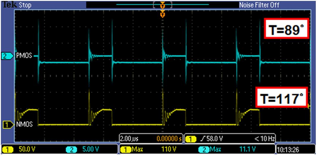
The case temperature of main FET is up to 117C at room temperature and full load condition. Thanks for your support!

Please find the attached schematic and waveforms.

Spec: 12V to 54V/2.3A

Schematic:
1. changed MP1/MP2/MP3 to FDMS86200 to cover 110V Vds spike.
2. changed MP4 to Si7461DP for lower conduction loss.

Schematic LM5026.pdf

MOSFET waveforms:

Best regards,

Sam Ting

  • Hi Sam,

    Have you calculated the power dissipation in the mosfets based on their RMS current and the device RDon at say 100C junction temperature ?

    You can use the TI power stage design tool, free down load on TI.com at,

    to calculate the voltage and current waveforms in the active clamp circuit.

    If you look at the TI power supply design seminar series there will be papers on calculating the switching loss in the mosfet,

    Regards

    Peter

  • Hi Peter,

    Thanks for your information! We want to add snubber to suppress the VDS spike at NMOS then we could choose better alternative NMOS for the design.

    Could you please share you experience how to add the snubber based on the schematic in attached? Thanks!

    Best regards,
    Sam Ting

  • Hi Sam,

    You can find this paper on snubber design on ti.com,

    One other thing you should look at is the fact that the Vds waveform on the main fets looks like its taking a long time to charge the clamp capacitors, this could be because the Coss of the three mosfet MP1, MP2 and MP3 are about 400 to 500pF each so they add another 1.5nF of capacitance to the circuit. You may want to remove CP11, 1.5nF and see if the waveform becomes more rounded. Please also check the layout and minimise the PCB trace lenght between the clamp components and the main fets.

    Regards

    Peter

  • Hi Team

    I will try the above suggestions and reply.

    Thanks~