This thread has been locked.

If you have a related question, please click the "Ask a related question" button in the top right corner. The newly created question will be automatically linked to this question.

LM350A: How does the CC/CV circuit work

Part Number: LM350A
Other Parts Discussed in Thread: LM317

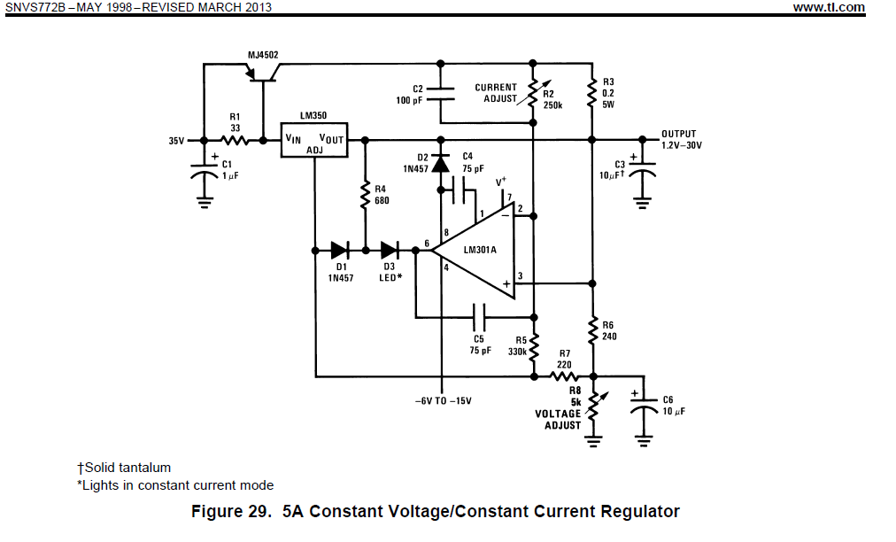
I have a few question about the circuit given below, taken from the application note referenced snvs772b page 12/21.

*How does teh LM301A controls the LM350 to acheive a 5A constant voltage/constant current regulator. in another word where is the voltage loop block and the current loop block.

The LM350 is designed to give 3A max.

*What is the role of D1 and D2 in tne analysis of the circuit ?

  • Hi Kirous,

    The voltage loop is formed by R6 and R8.
    The current loop is formed by the LM301A, R2 and R5.

    Diode D2 acts as a clamp to ensure the device is not over stressed.
    If pin 8 goes higher than the Vout by roughly 1V, the D2 will clamp the op-amp at this value.

    The capacitors in the circuit are for filtering and stability.

    Voltage Loop
    The voltage loop is the same as any adjustable converter.
    The output of the LM350 is sensed by resistors R6 and R8.
    These form a voltage divider, and the output of the voltage divider goes into the adjust pin of the LM350.

    Current Loop
    When the voltage divider formed by R2 and R5 produces a voltage on the inverting input of the Op-Amp which is lower than the output voltage, the Op-Amp will try to pull the output low.
    This will engage the current loop.  Altering R2 changes this current limit setpoint.
    When the current loop is engaged, the output of the LM301A pulls low and allows current to flow through the LED (D3).
    The resistor R4 provides the current limiting resistance for the diode, so it does not exceed any maximum limits.
    When the current loop is engaged, diode D1 is forward biased and the voltage on the adjust pin of the LM350 is regulated to maintain the designed current limit.

    Thanks,

    - Stephen

  • Thanks a lot for your reply

    It's ok for the voltage loop, but why there is R7 between the Adj pin and the divider output ? what is it for ?

    Please, could you be more specific about the current loop? why do we have used a pnp transistor and R3?

    How to get 5A from LM350 while the datasheet says that the maximum output current for LM350 is 4.5A .

  • Hi Kirous,

    R7 will limit the current that the Op-Amp will see during a catastrophic failure, and in the event that the Op-Amp is shorting its output to ground.  R7 will prevent the output capacitor from producing a large spike in current through the diodes and through the Op-Amp, potentially destroying this chain of circuitry.

    The PNP transistor is in parallel with the linear regulator (and, internal LDO pass element).
    When enough current flows through the 33 ohm resistor, the PNP will turn ON and share the load current with the linear regulator.
    This is a common technique to increase the load current ability of the linear regulator circuit.
    The LM350 is not rated for 5A, and may hit current limit no greater than 3A according to the datasheet.
    So to achieve 5A load current, the PNP will provide the extra current.

    The R3 resistor acts as a ballast resistor to aid in the current sharing of the LDO and PNP transistor.
    There are a number of Texas Instruments Reference Designs that go into this topic.
    Please see the following link for one such reference design example:

    http://www.ti.com/lit/ug/tidub16a/tidub16a.pdf

    Thanks,

    - Stephen

  • Hi expert

    What realy disturbed me, is that the current and the voltage loops share R8 and ADJ pin fo LM350 so I found difficulties in analysing the circuit. R3 is not a ballast resistor, but I believe that it is a sense resistor. The amplifier here is a type I error amplifier. It gets the error signal form the voltage across R3 but to what this voltage is comparend (What is the Vref of this EA) ? and why the two loops share R8 ?? 

  • Hi Kirous,

    I prefer to think of this Op-Amp as configured as an integrator.
    So it integrates the error across the input terminals.
    When you use terminology as "type 1" or "type 2", it typically means you are compensating something, but that's not what this configuration is doing.  However, you are correct - an integrator is also a "type 1" configuration.
    The Op-Amp is not sensing the voltage across R3, as there is another resistor in the way (R2).

    The "Vref" of this op-amp is the same as Vout.
    The inverting node is using a voltage divider based on Vin.

    The 0.2 ohm resistor is a ballast resistor.
    If the 0.2 ohm resistor were a sense resistor, then a current sense amplifier would be connected directly across it.
    The current sense resistor would also be directly in series with the output.
    That is not the case in this circuit.  The 0.2 ohm resistor is only in series with the PNP, but not the LDO output.
    And there is no current sense amplifier connected directly across the output.
    Additionally, 0.2 ohms is a very large value for a current sense resistor, especially when discussing an output load of 5A.
    You typically do not want to drop a lot of volts across a current sense resistor, which would significantly affect the electronics being powered by the LDO. 

    I hope this is helpful.
    As always, please let me know if I can be of any further help.

    Thanks,

    - Stephen

  • Hi Kirous,

    I missed your question on why the two loops share R8. 

    The parallel combination of R8 and C6 form a filter that is used to filter noise in the two loops.
    As the current loop gets closer to taking over control, random noise in the circuit or transients on the load can push it over the edge.
    The output of the current loop circuit goes into the adjust pin, which is really just another Op-Amp with high gain at low frequency.
    This can have the effect of forming a low frequency oscillation on the output.

    It is fine to connect R5 to GND but you will want to provide sufficient filtering another way, if noise or load transients can affect your design.

    Thanks,

    - Stephen

  • Thanks again Stephen! 

    You have clarified to me many things concerning this circuit, I have tried to simulate it in TINA TI V9, and the attached is the simulated circuit, but I did not get what I have expected 

    My specs are: 

    Vout = 5v

    Iout =2A

    Rload =Vout/Iout = 2.5ohm

    When Rload less than 2.5ohm, I expected the current loop to take control and when the Rload greater than 2.5ohm, the voltage loop should take control. But I did not get that.

    The diodes do not seem to be acting the circuit.

    Please could you give me the DC and AC transfer function of the current loop?? 

    Thanks 5A CC--CV regulator.TSC

  • Hi Kirous,

    There may be some issues with the simulation models that are causing some inaccuracies.
    The Op-Amp symbol has two nodes labeled pin 9, which is where the diode D2 would connect.
    That does not match with the schematic we have been reviewing.  The Op-Amp model may not be accurate.

    The LM317 model is definitely incorrect.
    I stripped out all of the circuitry except the basic LM317 model, which I reimported from TI.com, and the feedback resistors.
    The steady state solution is 5V but the adjust voltage is completely off.  It should be 1.25V, not 3.77V.
    The unencrypted netlist lists this voltage as 1.25V in the .PARAM statement, so it is not immediately clear if the issue is with TINA, the model, or both.

    Unfortunately, correcting the model is not a trivial task and is beyond the scope of the help I can offer here.
    I would try building this design on a breadboard or protoboard instead.
    Focus on the steady state results and get the DC voltage correct without worrying about the current loop.
    Then add in the current loop to get the results you are looking for.

    Thanks,

    - Stephen

  • Hi stephen

    Any updates about the circuit and its simulation ?

    Thanks

    Kirous

  • Hi Kirous,

    There may be some issues with the simulation models that are causing some inaccuracies.
    The Op-Amp symbol has two nodes labeled pin 9, which is where the diode D2 would connect.
    That does not match with the schematic we have been reviewing.  The Op-Amp model may not be accurate.

    The LM317 model is definitely incorrect.
    I stripped out all of the circuitry except the basic LM317 model, which I reimported from TI.com, and the feedback resistors.
    The steady state solution is 5V but the adjust voltage is completely off.  It should be 1.25V, not 3.77V.
    The unencrypted netlist lists this voltage as 1.25V in the .PARAM statement, so it is not immediately clear if the issue is with TINA, the model, or both.

    Unfortunately, correcting the model is not a trivial task and is beyond the scope of the help I can offer here.
    I would try building this design on a breadboard or protoboard instead.
    Focus on the steady state results and get the DC voltage correct without worrying about the current loop.
    Then add in the current loop to get the results you are looking for.

    Thanks,

    - Stephen