


Hi
Attached schematic as below.
1. This problem is encountered in mass production. It is not easy to reproduce at present, and no problems will occur under normal circumstances, so which parameters may not be designed reasonably.
2. The data obtained by the end customer, so what is reproduced now is similar to the phenomenon encountered by customers.
3. When the discharge port is disconnected, the AFE protection chip enters deep sleep, and CHG_EN and DSG_EN output low levels; when the discharge port is connected, the AFE protection chip wakes up from deep sleep, and CHG_EN and DSG_EN output high levels.
4. Test method: Plug and unplug according to the set frequency on the plug-in machine. Light load is always on.

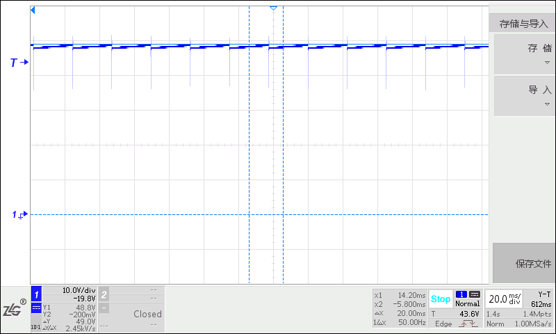
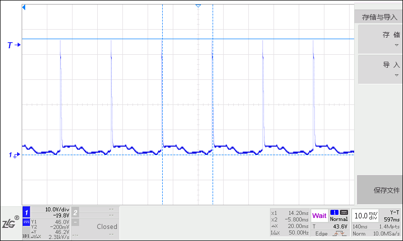
5. Capture the voltage waveforms of the VDDCP, PACK, CHG, DSG pins on the BQ76200 (the ground of the oscilloscope probe is all connected to the battery pack B-), and the Voltage waveform. The time interval from the waveform is 20ms.
6. I have checked the temperature and voltage characteristic curve of the 2.2uf capacitor on VDDCP, and combined with the test situation, the influence of the capacitance change of the temperature capacitor can be basically eliminated; there is no leakage of the 16V voltage regulator tube between the GS pin of the discharge MOS In some cases, the MOS hiccup phenomenon still exists after the voltage regulator tube is removed, and the universal transformer string cannot detect the current on the voltage regulator tube circuit.
This internal block diagram (especially the red circle) does not read the working mechanism in the document. Can you help explain what possible reflow paths can cause this phenomenon that we caught, and what can be solved method?

Waveforms at various points during abnormal times (all probes are connected to the B-test):
PACK waveform
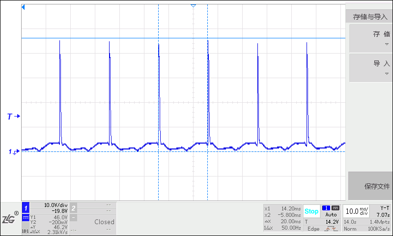
B+/B waveform

CHG pin voltage (CHG_EN normally outputs 11V at this time)
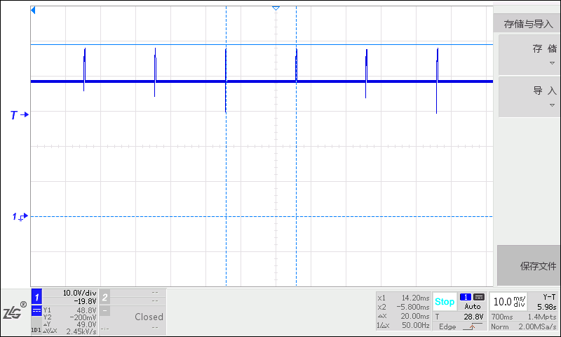
DSG pin voltage (CHG_EN normally outputs 11V at this time)
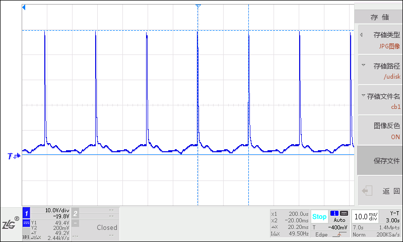
VDDCP pin voltage
P+/P- voltage
Waiting for your reply
Thanks
Star
