Hi team,
My customer has some question about our PFET choose suggestion as below description in our datasheet.
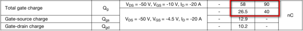
- What is the function of Cf capacitor which is putting between Vin pin and Vcc pin? Is it for the frequency response of LDO? Customer would like to know whether there is any side effect since removing it at PFET Qg>30nC and why it will improve the peak current detection performance since it is removed?
- Why can it also improve the peak current detection performance since CF be connected from the VCC pin to the CSN pin?
Customer would like evaluate which way is more suitable for their mass-production product. Thanks.