This thread has been locked.

If you have a related question, please click the "Ask a related question" button in the top right corner. The newly created question will be automatically linked to this question.

TPS54360B-Q1: TPS54360DDAR

Part Number: TPS54360B-Q1
Other Parts Discussed in Thread: ALLIGATOR, TPS54360, TPS54360B

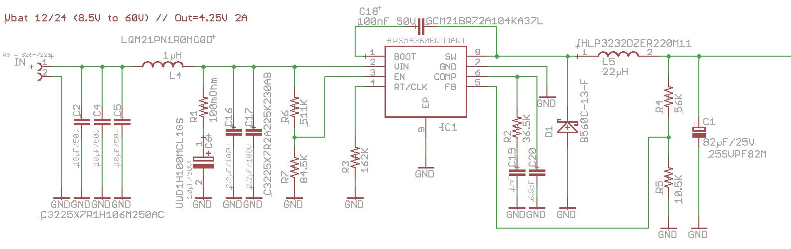
Hi Team. I've designed a DC-DC converter using WEBENCH and TPS54360B-Q1.

I've not found exactly that part from the providers and then I've used TPS54360DDAR. The circuit behave correctly in terms of regulation and programmed voltage output and UVLO.

But even if using the parts suggested from WEBENCH, I'm experiencing bad results on the Vout in terms of noise.

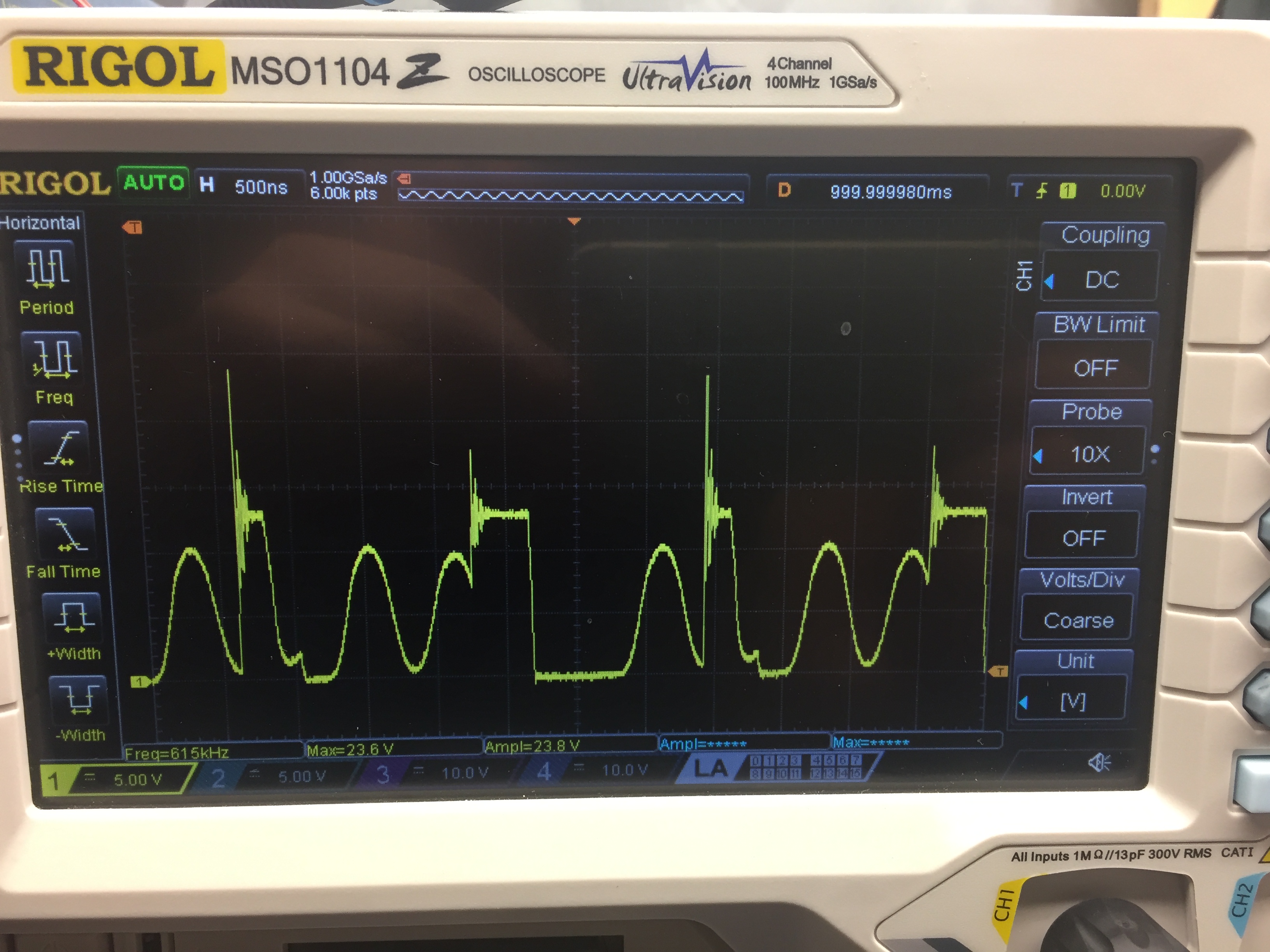
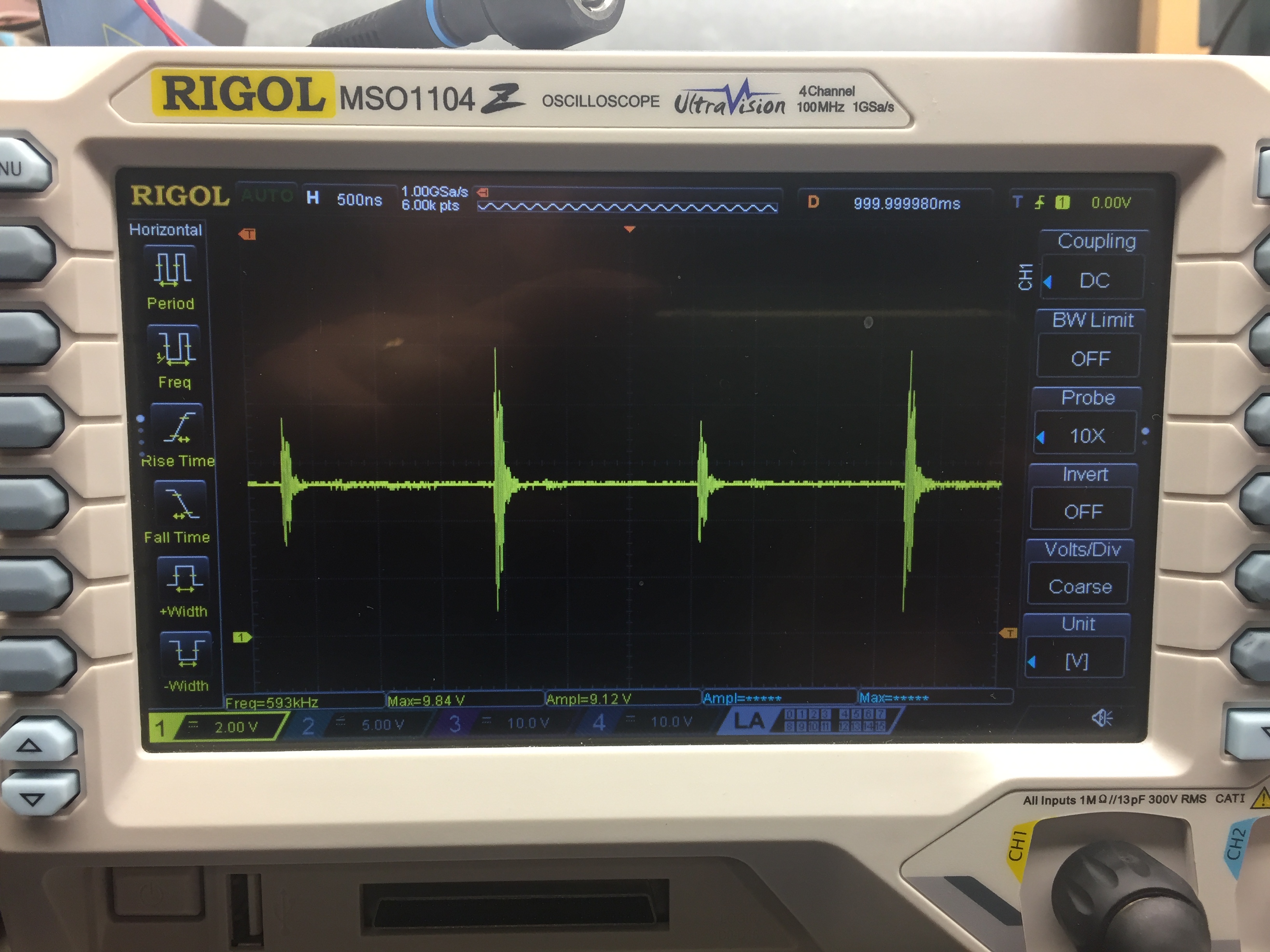
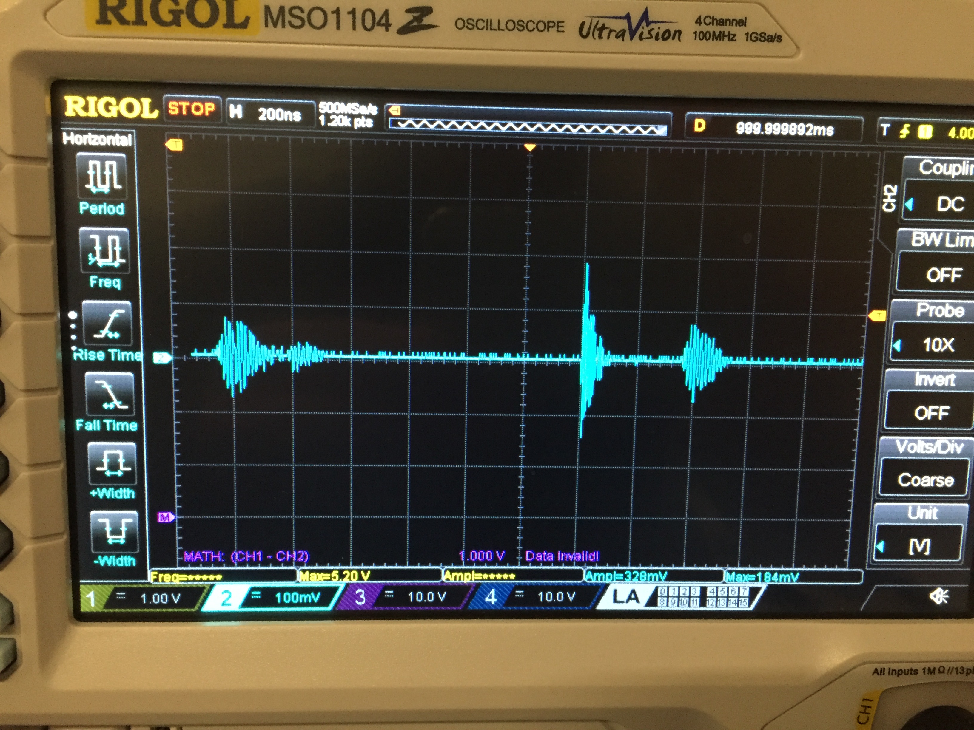
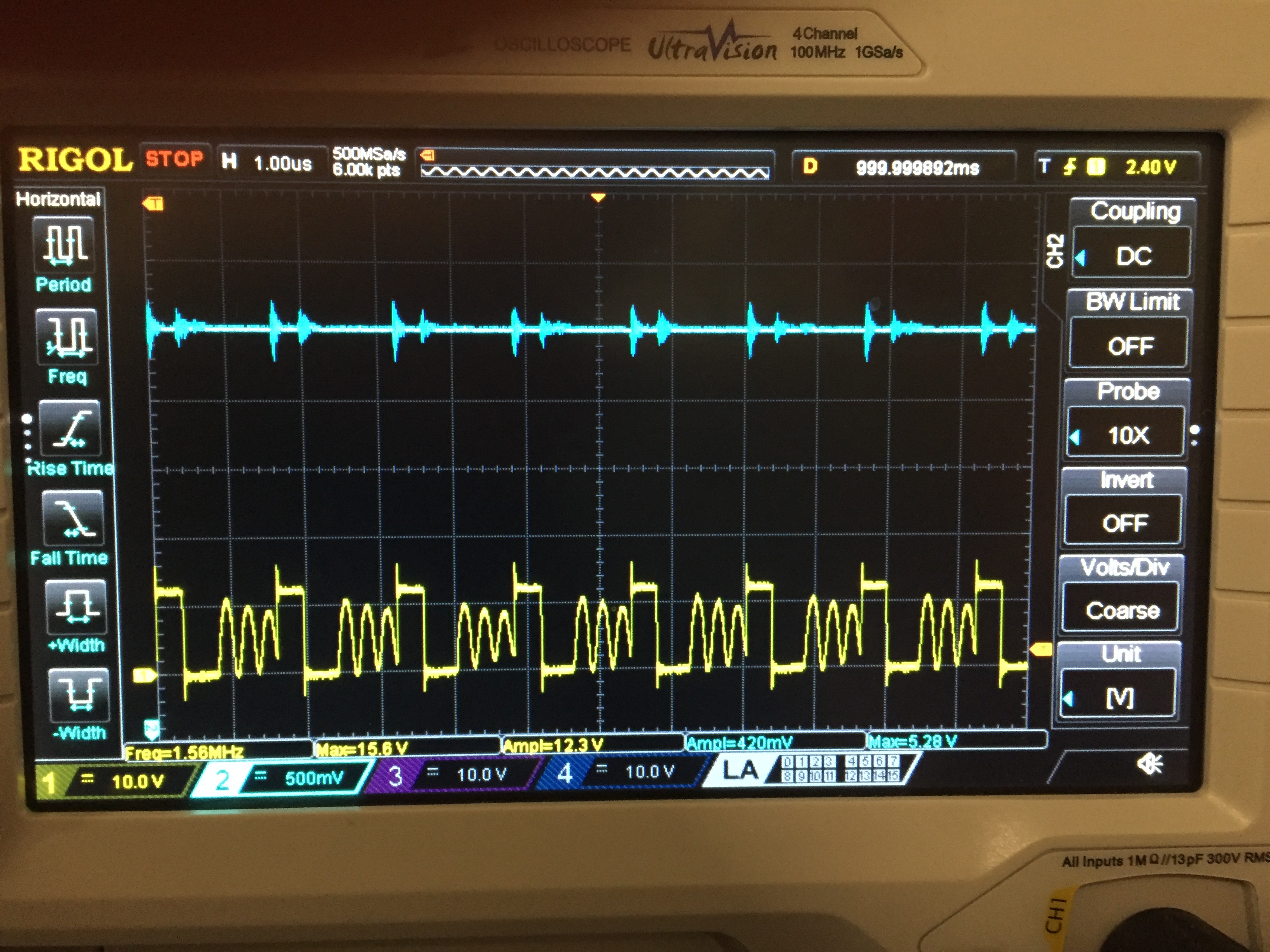
As you can see from the included pictures, the voltage at the output is affected by a huge noise sometimes in terms of some volts!

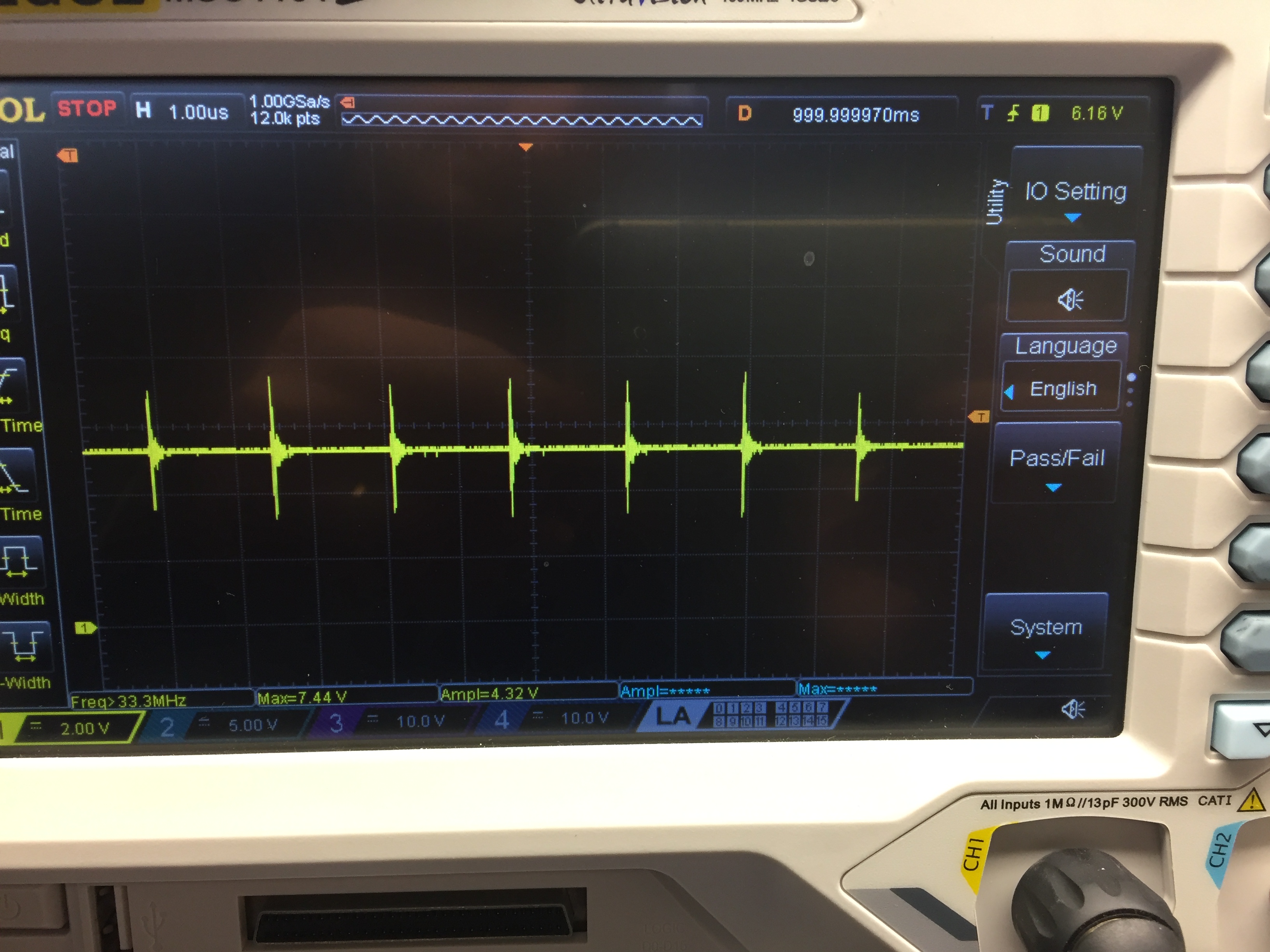
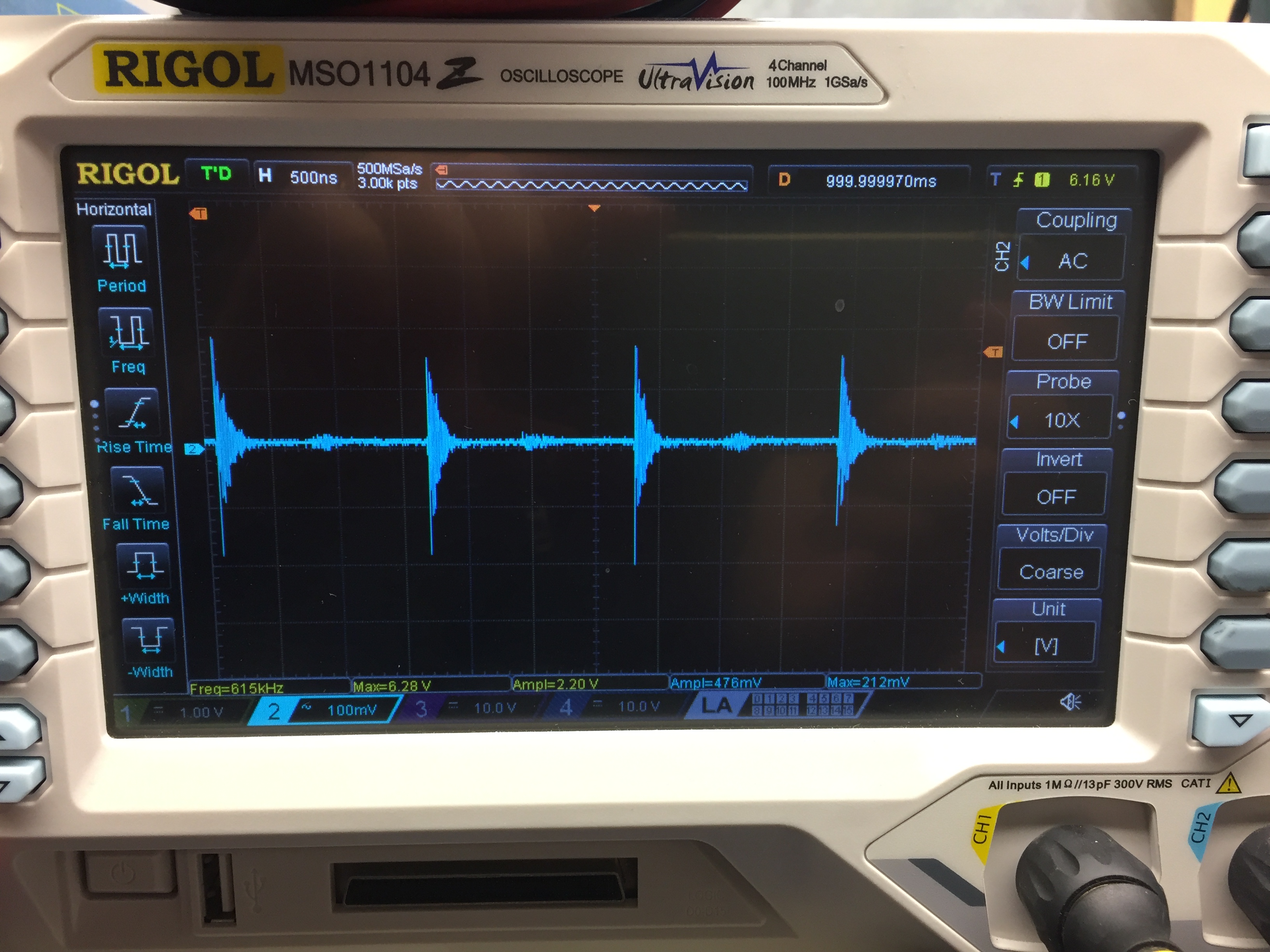
I've tested the circuit using the following parameters: Vin = 12V; Load=10mA; Vout=5.06V.

The picture named "TestPoint1.jpg" show the wave at the cathode of the catch diode (5V/div on the scope)

The picture named "TestPoint_Out.jpg" show the wave at the output capacitor (C1) (2V/div on the scope)

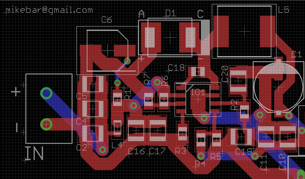
I've included the schematic used (with manifacturer pat number) and also the PCB layout.

The capacitor C1 is an electrolytic one (suggested by WEBENCH 82µF 28mOhm ESR, Panasonic part no. 25SVPF82M).

The questions are:

- there is a difference between TPS54360B-Q1 and TPS54360DDAR that can cause the problems you can see in the pictures?

- If there aren't so much differences, what can cause the behaviour as seen in the pictures?

Can you suggest please what to fix?

Thank you for your support.

Best regards.


Test Point1.jpg:


Test Point_Out.jpg:


  • TestPoint1.jpg

    TestPoint_Out.jpg

    PCB Artwork

    Schematic

  • Hi Michele,

    Thanks for the comprehensive post.

    You are seeing some high frequency noise it looks like.

    Are C10 and C11 populated? I see them in the layout, but dont see them in schematic entry.

    Can you remove the scope probe tip and alligator clip and do tip and barell measurement across output capacitor? Long lead will have transformer coupling and additional inductance with high di/dt currents.

    Please see 16th minute of this video. There is some good information if you have time to watch more.

    You could also experiment with placement of input capacitors closer to the IC to reduce HF noise if still present, if measurement technique cannot be improved.

  • Thank you for your quick feddback.

    C10 and C11 are populated. Actually I've uploaded only the relevant portion of the schematic. Below you will see the ful schematic.

    There is also a DC-DC converter for ground splitting and related EMI filter.

    So, the capacitors C10 and C11 ideally belong to the TMR2 EMI filter, while the waveforms I've sent you in the pictures are collected across C1.

    I'll ask right now to somebody at my Lab to do the tip & barrell measurement across C1, just to avoid the transformer coupling you're talking about.

    However, that video is very helpful. I'll go to see it from beginning to the end. Thank you very much.

    Best regards,

    Michele.

  • Thanks for sharing.

    Please let us know the outcome of the experiments.

  • Dear Marshall Beck,

    as promised I've done the measurement as suggested, but no luck.

    PLEASE NOTE THAT ALL THE TESTS has been done with Vin=12VDC (from a linear power supply), 100mA  load

    As you can see from the picture 1, this is the result with Tip&Barrell measurement: Please note the scale: It is set to 2V/div.

    Then I've changed the diode proposed by the Webench (B560C) with another one: MURS320. You can see from the following picture that the noise is still there, but greatly reduced: the scale now is set to 100mV/div:

    Then I've changed also the inductor: from the Webench's proposed one (22µH) to a 5.8µH one. Again it seems a better result, but the noise is still there:

    Following are the final measures as per the previous setup:

    The blue wave is across C1 of my schematic (directly on the output of the TPS54360) (500mV/div)

    The yellow wave is from the cathode of the catch diode. (10V/div)

    The waveforms I'm getting are close enough to the ones describe into the datasheet, except some peak.

    The frequency is around 620 kHz, that should be the switching frequency of the regulator.

    Questions are:

    - Is that kind of output something acceptable from this type of regulator?

    - Is that kind of output safe enough to power microcontrollers?

    - Is that noise affecting the EMI conducted/radiated tests, even if there is an input filter that should be good enough to stop it?

    - There is something more I can do to eventually reduce that noise, if it's really needed?

    Thank you very much for your support and help.

    Best regards,

    Michele.

  • DC regulators can be low-noise with proper design, but I guess that is relative.

    Figure 39 in TPS54360B shows typical output ripple for light load condition.

    Proper placement of high frequency input caps can affect conducted EMI. Often, SW node ringing is affected by placement of these caps. With asynchronous power converters, passing EMI becomes more difficult in comparison to synchronous converters, as more parasitics are introduced. 

    Hight frequency noise can be filtered out for very stringent power supply requirements, for that of instrumentation equipment, though, powering a micro controller, the micro controller should be able to tolerate some high frequency content on the supply.

    A few comments on your experiments.

    In general, for a given inductor, a smaller inductance value for a similar family of inductors will have a higher self resonance frequency. This will result in ability to better filter out higher order harmonics of switching frequency, as well, broad band high frequency noise.

    In regards to diode selection, I would think the equivalent capacitance of the diode would effect how much energy can be stored in it. When the diode snaps backs the energy comes out of the diode. This recovery can cause some noise on the output. How the diode snaps back, will effect efficiency and noise. You could try adding a boot resistor in series with cboot cap to slow down turn on of high side fet, but this will increase switching loss.

    These are some things to think about.

    Happy new year.

  • Thank you very much for your detailed answer.

    Do you have please some suggestion about the value to start with for the resistor to use in series with CBoot ?

    Best regards and happy new year you too.

    Michele.

  • I would start with 10ohm. Anything above 50ohm I would think you would see a big hit to efficiency and then eventually with a big enough boot resistor run into a situation in which boot UVLO is hit, do to the fact that the boot cap doesn't have enough time to charge up to its required voltage (SW to BOOT voltage) to turn on the highside.