This thread has been locked.

If you have a related question, please click the "Ask a related question" button in the top right corner. The newly created question will be automatically linked to this question.

TPS54260: Power chip tps54260dgq failure event

Part Number: TPS54260


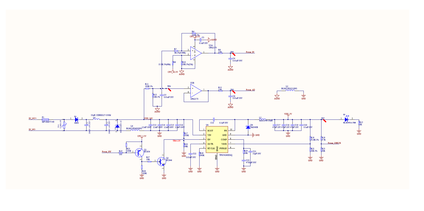
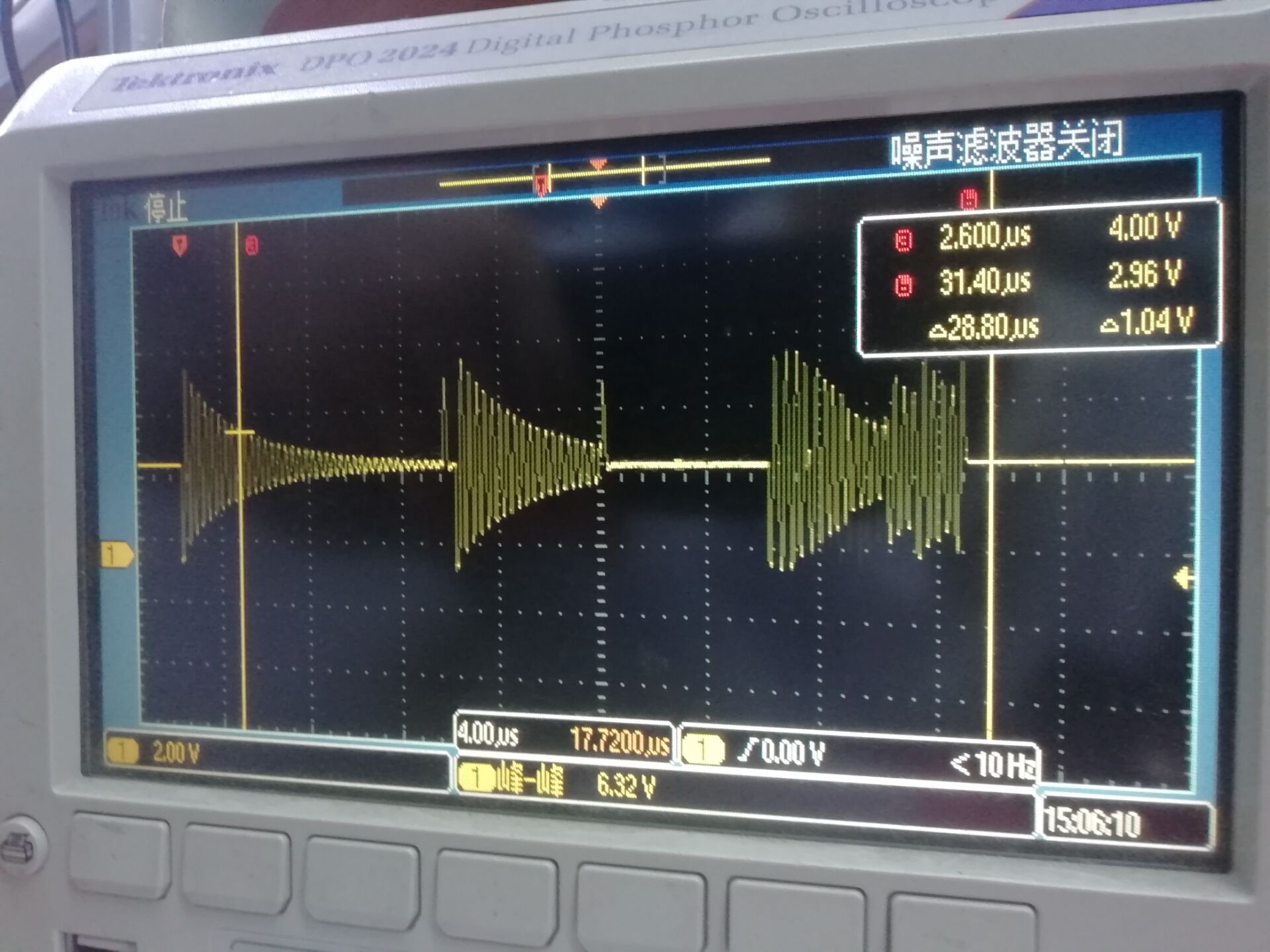
Recently, There were 6 pcs failure of tps54260dgq power supply chip in 24 V power supply system. After measurement, the output voltage of the power

supply chip was only 2.5V (5V normally), After replacing tps54260dgq of the product in question, 5V voltage can return to normal. What are the possible

causes the tps54260dgq failure. The attachment is its application circuit diagram  Please help to check  if there is any problem。

  • Wilson,

    What is the maximum input voltage on the 24V rail?

    I see a couple of issues with the input power.

    1) You need a capacitor with ESR at VIN to provide damping to input pi filter. Otherwise you can have LC resonance and the VIN node will be unstable.

    See http://www.ti.com/lit/an/snva538/snva538.pdf 

    2) Why do you have an inductor seperating the chip GND and the power GND? I think that will cause more resonance issue and also make the VIN voltage less predictable during turn-on, and could also potentially force the GND node negative during a turn-off.

    Please clarify,

    -Orlando

  • Hi Mr.Orlando

    Thank you for your advice ,For this failure , we make a Comparison document to show the every pin's waveform of TPS54260 between Normal product and Fault product.


    Please help to confirm whether the problem you see a couple of issues with the input power is related to this failure. 

    in addition Reply to your questions as follows

    1) the maximum input voltage is 24V.


    2) Why do you have an inductor seperating the chip GND and the power GND? You should mean the Magnetic beads L6 in Circuit diagram. this bead may be helpful for products to pass EMC conduction test

    TPS54260 Pin status comparison - .pdf

  • Hi  Mr Orlando:

    Is this problem related to the frequency setting of the power supply chip.   At present, I found that the chips work frequency with problems are all  set to 500KHz (R26=240Kohm)before changing the frequency. The

    current frequency is set to  270khz(R26=470Kohm).

  • Wilson,

    I still think it is enough damping to the input pi filter.

    Currently the input PI LC filter will have undamped resonance behavior, and this uncontrolled resonance can end up damaging the device.

    Please see http://www.ti.com/lit/an/snva538/snva538.pdf for how to damp the input pi-filter.

    -Orlando

  • Hi Ms Orlando 

    thank you  Have you seen the document  TPS54260 Pin status comparison - .pdf 。please help  me to comfirm Whether the down stroke waveform at the red

    circle will damage IC in pH pin. Can you give me some suggestions for improvement

  • Willson,

    That ringing is normal behavior. It is a function of parts that run in Discontinuous Conduction Mode (DCM).

    Right now the output current is less than 1/2 the inductor ripple current, so the inductor current can go to zero in one cycle.

    For best light-load efficiency we prevent negative inductor current by turning off the low-side MOSFET, and the SW node will ring as an LC due to SW node capacitance and buck inductor.

    You can see similar behavior in Figure 54 on page 37 on the datasheet, it is nothing to worry about and how the part is working.

    Hope this helps,

    -Orlando

  • Hi  Orlando

    I have new found I measure voltage  of the boot-pH between the failed chip and good chip .we found the failed chip boot-pH voltage is 3.2V and the good chip boot-pH voltage is 6.14  .so I know that the failed chip tps54260dgq boot pin voltage is pulled low.Then I short circuit  the boot pin and vin pin to increase the boot pin voltage to vin=12V. A miracle happened the failed chip out voltage is back from 2.5v to 5V. when i open  circuit  the boot pin and vin pin ,some tps54260dgq chip back to 2.5V or 3.2V  and one tps54260dgq chip  remain at 5V .  and  I tested the resistance to ground of each pin,The good IC  and the bad  IC are the same

    I can't even tell if the IC's broken  and why the voltage of ss/TR Pin and Vsense are 0.46V    Comp pin is 1.89V   How to understand the following sentence  in the datasheet.

    The error amplifier output is compared to the high-side power switch current. When the power switch current reaches the level set by the COMP voltage, the power switch is turned off. The COMP pin voltage will increase and decrease as the output current increases and decreases. The device implements a current limit by clamping the COMP pin voltage to a maximum level 

    The accessory is the waveform of boot  pin  

  • Willson,

    Looking at the block diagram (Section 7.2 pg12) It seems like the Boot Charge sub-circuit connected to VIN has been damaged.

    It also appears the EN is being reset (16Hz). Is that from the external logic?

    If its not external logic then the internal shutdown logic could be damaged and triggering that 16Hz reset.

    The IC is definitely broken. Maybe you can test the resistance between Boot-VIN to confirm?

    Also SS is charged by a Current Source (from VIN) to charge the SS capacitor.

    Since SS is not rising the current source also appears damaged.

    Current mode control modulates the inductor current to control output voltage.

    The Comp node is the output of the error amplifier which is (Reference voltage - Sense voltage) . You can see this in the block diagram.

    Comp is higher on the damaged part because the Sense voltage is way below the reference voltage and the controller wants to keep the power switch on to  let more current through to bring up VOUT (and bring up Sense).

    The boot pin voltage should not look like that. 

    I still think the root cause is not enough damping to the input pi filter.

    When the undamped resonant VIN is presented to the IC  the high frequencies could damage the boot charge circuit and/or the current sources.

    This will be significant at load transients where the output current changes quickly, and also line transients, where the input voltage changes quickly.

    I suggest you add a damping capacitor with ESR (or a series resistor) as the previous appnote suggested.

    -Orlando