This thread has been locked.

If you have a related question, please click the "Ask a related question" button in the top right corner. The newly created question will be automatically linked to this question.

TPS51200: Power domain of TPS51200

Part Number: TPS51200

Hi,

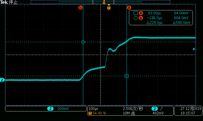
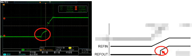
The following figure shows that when the power is turned on, we find that the startup waveform of the REFOUT pin of the chip has a backlash. Is this startup waveform normal? If not, please reply:
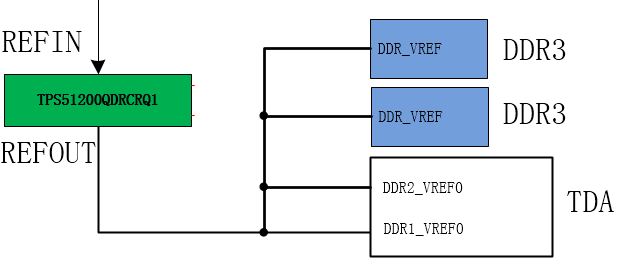
1. Attachment is the TPS51200 schematic diagram , please do a schematic diagram verification
2. The MOSFET discharge circuit has been integrated inside the REFOUT pin. We want to know under what circumstances we need to discharge to the GND pin through an external MOSFET?

design20.pdf

  • Hello, 

    REFOUT follow REFIN when REFIN is above 0.39V. REFIN follows VDDQ/2. 

    Can you probe VDDQ(1V35_DDR), REFIN, REFOUT waveforms at the same time?

    Also, can you remove R303 and R307 in your schemaic and check the REFOUT waveform? The purpose is to check if the REFOUT backlash is caused by external circuit. 

    No external discharge circuit is needed for REFOUT. 

    Thanks

    Qian

  • A1:

    The system architecture is as follows,  VDDQ (1V35_DDR), REFIN, REFOUT waveforms are powered on at the same time, the REFIN waveform is normal.

    Q1:The REFOUT waveform is different from the manual. What is the reason for the rotation angle in the red circle in the figure below?

    Q2:

    Does the VO pin require an additional discharge circuit ?

  • Hello, 

    Q1, The initial REFOUT waveform could be caused by leakage current from DIMM side. That's why I suggest to remove R303 and R307 to confirm. 

    Q2, Usually additional discharge circuit is not needed for VO (VTT). However, if there is large VTT leakage current from DIMM side when TPS51200 is in off status, a bleeding resistor between VTT and ground is suggested to discharge leakage current and keep VTT voltage low. 

    Thanks

    Qian